ALLPCB


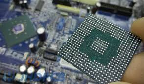
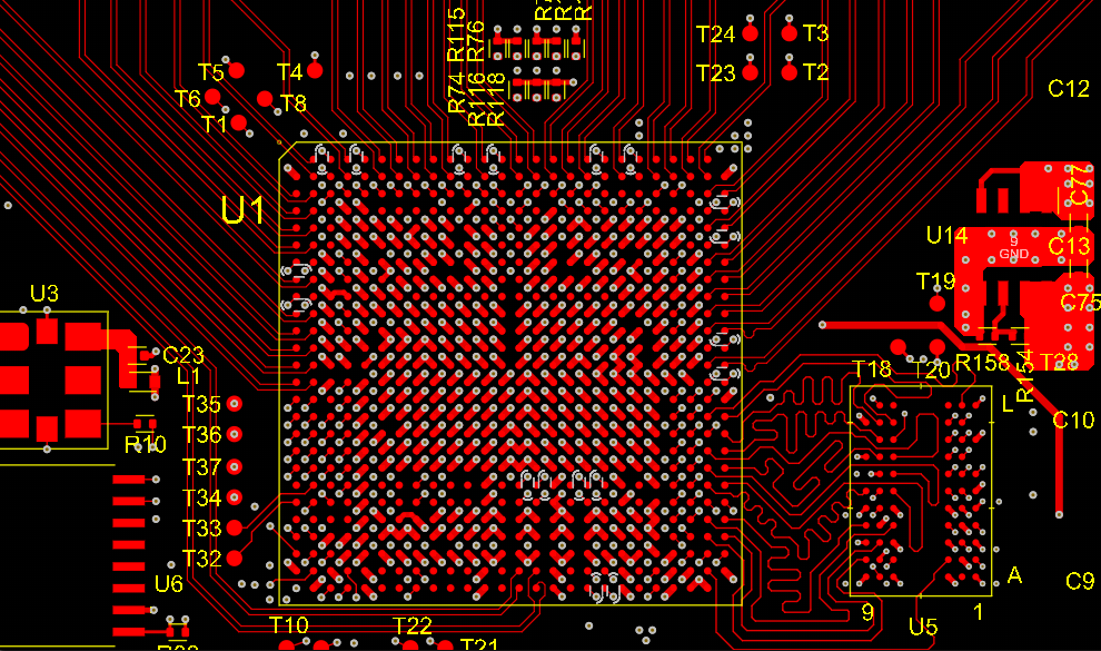
Ball Grid Array (BGA) packages have become a cornerstone of modern electronics, enabling compact designs with high pin counts for microprocessors, FPGAs, and memory devices. However, their dense pin arrangements pose significant challenges for PCB designers, particularly when it comes to escape routing—the process of routing signals from BGA pads to the rest of the board. As pin pitches shrink to 0.5 mm or less and pin counts climb into the thousands, effective escape routing becomes critical to ensure signal integrity, manufacturability, and performance. In this blog, we explore proven escape routing techniques for high-density BGA packages, offering practical insights for engineers tackling these complex designs.
Our goal is to equip you with actionable strategies to navigate the intricacies of BGA escape routing. From fanout strategies to via optimization, we'll break down each approach with specific examples and data to help you achieve robust PCB layouts.
Understanding BGA Escape Routing Challenges
High-density BGA packages, with pin counts often exceeding 1,000 and pitches as tight as 0.4 mm, create a complex routing environment. The primary challenge lies in escaping signals from the dense grid of solder balls to the PCB's outer layers or internal routing channels without causing congestion, crosstalk, or impedance mismatches. For instance, a 0.5 mm pitch BGA with a 40x40 grid contains 1,600 pins, requiring meticulous planning to route each signal while maintaining a trace width of 3 mils or less to avoid overlap.
Key challenges include:
- High Pin Density: Limited space between pins restricts trace routing, often necessitating micro-vias or high-density interconnect (HDI) techniques.
- Signal Integrity: High-speed signals, such as DDR4 interfaces operating at 3.2 Gbps, demand controlled impedance (typically 50 ohms) and minimal stub lengths to prevent reflections.
- Layer Count Constraints: Routing all signals may require multiple PCB layers, increasing costs unless optimized.
- Manufacturing Limits: Trace widths below 3 mils or via sizes smaller than 8 mils may exceed standard fabrication capabilities, requiring advanced processes.
To address these, engineers must adopt strategic escape routing techniques tailored to the BGA's pitch, pin count, and signal requirements.
Key Escape Routing Techniques
1. Dog-Bone Fanout for Larger Pitch BGAs
The dog-bone fanout is a widely used technique for BGAs with pitches of 0.5 mm or greater. In this approach, each BGA pad connects to a via through a short trace resembling a dog bone, allowing signals to transition to inner PCB layers for further routing. This method is effective for mid-range pitch BGAs (0.5–1.27 mm) because it provides enough space to route one or two traces between adjacent pads.
How It Works:
- Outer - Outer rows of BGA pads are routed directly outward with horizontal or vertical traces.
- Inner rows use vias placed between four adjacent pads, connected via diagonal traces.
- Typical trace widths are 3–4 mils, with clearances of at least 0.1 mm for a 0.65 mm pitch BGA, ensuring manufacturability.
Example: For a 0.8 mm pitch BGA with 400 pins, the outer two rows (approximately 80 pins) can be routed without vias, while inner pins use dog-bone vias to reach a second signal layer, reducing congestion.
Pros: Simple to implement, compatible with standard PCB manufacturing, and reliable for larger pitches.
Cons: Ineffective for pitches below 0.5 mm due to insufficient space for traces and vias.
2. Via-in-Pad for Fine-Pitch BGAs
For BGAs with pitches below 0.5 mm, via-in-pad technology becomes essential. Here, vias are placed directly within the BGA pads, filled with conductive or non-conductive epoxy, and plated over to create a flat surface for soldering. This maximizes routing space, allowing signals to escape vertically to inner layers.
How It Works:
-
Micro-vias, typically 8 mils in diameter with a 4 mil hole, are drilled into BGA pads.
-
Vias are filled to prevent solder wicking, ensuring reliable joints during reflow.
-
Signals are routed to inner layers, where wider traces (e.g., 5 mils) can be used to reduce resistance.
Example: A 0.4 mm pitch BGA with 1,000 pins might use via-in-pad for all inner pins, with micro-vias connecting to a high-density routing zone with 3 mil traces and 3 mil spacing. This setup supports high-speed signals like PCIe 4.0, requiring 85-ohm differential pairs.
Pros: Maximizes routing density, ideal for ultra-fine pitches, and supports HDI designs.
Cons: Increases manufacturing complexity and cost; requires advanced PCB fabrication capabilities.
3. Staggered and Ordered Escape Routing
For complex designs, staggered or ordered escape routing optimizes signal paths and reduces crossover. Staggered pin arrays, where pins are offset at 60-degree angles, increase spacing between pads, easing trace routing. Ordered escape routing, often solved using algorithms like Min-cost Multi-commodity Flow (MMCF), ensures signals exit the BGA in a specific sequence to avoid conflicts.
How It Works:
-
Staggered arrays allow wider traces (e.g., 4 mils) between pins, reducing crosstalk.
-
Ordered routing uses algorithms to assign vias and traces, minimizing wire length and congestion.
-
Software tools like Allegro PCB Designer or Altium Designer automate these processes, applying constraints for impedance and spacing.
Example: In a 1,200-pin BGA with a 0.65 mm staggered pitch, ordered routing might assign power and ground pins to the outer rows, high-speed signals to the next layer via micro-vias, and low-speed signals to deeper layers, achieving 100% routability with total wire length reduced by 15% compared to manual routing.
Pros: Enhances routability, reduces crosstalk, and supports automated design flows.
Cons: Requires advanced software and expertise; computationally intensive for large BGAs.
4. HDI and Micro-Via Optimization
High-density interconnect (HDI) techniques, combined with micro-vias, are critical for ultra-high-pin-count BGAs. HDI boards use multiple layers with fine traces (2–3 mils) and micro-vias to create compact routing channels, reducing layer count and cost.
How It Works:
-
Blind or buried micro-vias connect specific layers, minimizing stub lengths.
-
Layer stackups are optimized, e.g., a 12-layer board with 4 signal layers dedicated to BGA routing.
-
Signal integrity tools simulate impedance (e.g., 50 ohms single-ended) and crosstalk, guiding via placement.
Example: A 2,000-pin BGA for a 5G baseband processor might use an HDI board with 3 mil traces, 8 mil micro-vias, and a 10-layer stackup. Signal integrity analysis ensures that 28 Gbps SerDes signals maintain eye diagram integrity.
Pros: Supports extreme pin density, improves signal integrity, and reduces board size.
Cons: Significantly increases fabrication costs; requires precise design validation.
Best Practices for BGA Escape Routing
To maximize success, consider these practical tips:
- Plan Early: Collaborate with your PCB manufacturer to confirm capabilities (e.g., minimum via size, trace width). For instance, confirm if they support 8 mil micro-vias with 4 mil holes for via-in-pad designs.
- Optimize Layer Stackup: Allocate specific layers for high-speed signals, power, and ground. A typical 10-layer stackup might dedicate layers 2 and 9 for BGA escape routing.
- Use Simulation Tools: Perform signal integrity analysis to verify impedance (e.g., 100 ohms for differential pairs) and minimize crosstalk (target < -30 dB at 5 GHz).
- Designate Routing Zones: Create keepout zones around BGAs to prevent component placement from blocking escape routes.
- Test Routability: Use PCB design software to simulate escape routing before fabrication, ensuring 100% routability without manual rework.
How ALLPCB Supports Your BGA Routing Needs
At ALLPCB, we understand the complexities of designing high-density BGA packages. Our advanced manufacturing capabilities, including support for HDI boards, micro-vias, and fine-pitch trace widths down to 2.5 mils, ensure your escape routing designs are fabricated with precision. With quick-turn prototyping, global logistics, and expert DFM (Design for Manufacturability) reviews, we help engineers bring complex PCB layouts to life efficiently and reliably. Whether you're routing a 1,000-pin BGA for a 5G module or a 400-pin FPGA, ALLPCB's services streamline your path from design to production.
Conclusion
Escape routing for high-density BGA packages is a challenging but manageable task with the right techniques. By leveraging dog-bone fanouts, via-in-pad technology, staggered/ordered routing, and HDI methods, engineers can achieve robust, high-performance PCB designs. Combining these strategies with early planning, simulation, and collaboration with your PCB manufacturer ensures signal integrity, manufacturability, and cost efficiency. As BGA packages continue to evolve, staying informed about these techniques will keep your designs at the forefront of innovation.