 ALLPCB


Introduction
In the PCB assembly process, selecting the appropriate soldering method directly impacts assembly quality, yield rates, and overall reliability. Reflow soldering and wave soldering represent two primary techniques, each suited to different component types and production needs. Reflow soldering excels with surface-mount technology (SMT) components, while wave soldering aligns better with through-hole (THT) assemblies. Understanding the reflow soldering vs wave soldering differences helps engineers optimize their manufacturing workflow. This soldering methods comparison explores technical principles, practical applications, and troubleshooting to guide your decision-making. Factors like board complexity, volume, and mixed-technology designs play key roles in choosing between reflow soldering equipment and wave soldering equipment.
What Is Reflow Soldering?
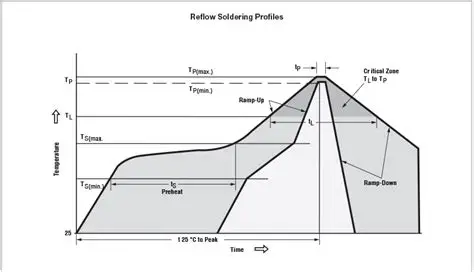
Reflow soldering involves applying solder paste to PCB pads, placing SMT components, and then heating the assembly in a controlled oven environment. The process melts the paste, forming reliable joints as it cools. This method supports high-density boards with fine-pitch components, common in modern electronics. Reflow ovens feature multiple heating zones to ensure uniform temperature profiles across the board. Engineers must profile the oven to avoid defects like tombstoning or bridging. Compliance with standards such as JEDEC J-STD-020E ensures proper handling of moisture-sensitive devices during reflow.
The solder paste, a mixture of flux and alloy particles, activates during preheat to clean surfaces and promote wetting. Precise control prevents overheating, which could warp boards or damage components. Reflow suits low- to high-volume production due to its flexibility with automation. Troubleshooting often focuses on paste viscosity and stencil alignment for consistent deposits.
What Is Wave Soldering?
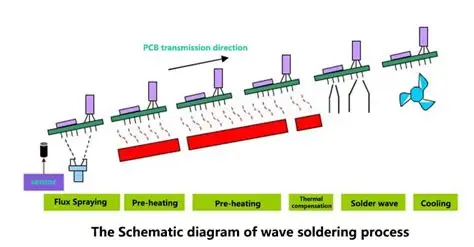
Wave soldering prepares through-hole components by fluxing the board, preheating it, and then dipping leads into a molten solder wave. The wave, generated by a pumped solder pot, contacts the underside of the board briefly to form joints. This technique thrives in assemblies with radial or axial leads, where mechanical strength is prioritized. Wave soldering equipment includes fluxers, preheaters, and solder pots with titanium liners for durability. The process demands careful dross management to maintain solder purity.
Preheating reduces thermal shock and activates flux for oxide removal. After wave contact, the board cools, solidifying joints. This method proves efficient for high-volume THT production but struggles with closely spaced SMT parts due to solder bridging risks. Regular maintenance of the solder bath temperature, typically around 250°C for SnPb or lead-free alloys, prevents issues like icicles or insufficient fill.
Reflow Soldering vs Wave Soldering: Key Differences
- Component Type: Reflow — Primarily SMT (fine-pitch capable); Wave — Primarily THT (through-hole leads).
- Solder Application: Reflow — Paste printed via stencil; Wave — Flux + molten solder wave.
- Heat Source: Reflow — Convection/infrared oven zones; Wave — Solder pot + preheat tunnel.
- Board Orientation: Reflow — Top-side components, bottom heating; Wave — Bottom-side immersion.
- Best For: Reflow — High-density, mixed-tech (SMT first); Wave — Simple THT, high-volume.
- Common Defects: Reflow — Tombstoning, voids, warpage; Wave — Bridging, icicles, solder balls.
This soldering methods comparison highlights SMT vs through-hole compatibility as a core distinction. Reflow offers precision for miniaturized designs, while wave provides robust mechanical bonds. Production speed varies; reflow handles complex boards slower per panel but scales with pick-and-place lines. Wave excels in throughput for pin-in-paste or glue-supported hybrids.
Technical Principles Behind Each Method
Reflow soldering relies on phase changes in solder paste driven by a thermal profile with distinct phases: preheat ramps temperature gradually to evaporate solvents, soak activates flux evenly, reflow peaks above liquidus for wetting, and cooling solidifies joints. Convection heating ensures uniform airflow, minimizing shadows from tall components. Profile optimization prevents intermetallic growth, which could embrittle joints over time.
Wave soldering uses capillary action as molten solder wets fluxed leads and pads during brief immersion, typically 3-5 seconds. The laminar wave design reduces turbulence and splashing, promoting even fill in vias. Preheat, often via IR or hot air, matches the board's thermal mass to the wave temperature, avoiding cracks from rapid quenching. Flux selection, water-soluble or no-clean, influences residue cleanup post-process.
Both methods demand alloy compatibility; lead-free SAC305 requires higher peaks in reflow (around 260°C) compared to wave's stable bath. Thermal gradients cause warpage in large panels, addressed by fixture design or low-CTE materials.
Advantages and Disadvantages
Reflow soldering advantages include superior joint uniformity on double-sided boards and compatibility with BGA packages, reducing manual rework. It minimizes handling damage since components stay secured by paste. However, it risks head-in-pillow defects if paste volume mismatches component size, demanding precise printing.
Wave soldering delivers strong THT joints with excellent hole fill, ideal for connectors enduring vibration. Setup is straightforward for prototypes, with lower initial costs for simple lines. Drawbacks involve contamination from solder drag-out on topside and limitations with fine-pitch SMT, often requiring selective pallets.
In mixed assemblies, reflow SMT first, then wave THT, but glue or pin-in-paste prevents component fallout. Cost-wise, reflow scales better for complexity, while wave suits volume THT.
Best Practices for PCB Assembly Process
For reflow, validate thermal profiles using thermocouples per JEDEC J-STD-020E to classify components by MSL levels. Bake boards pre-assembly to remove moisture, and use nitrogen atmospheres for oxide-free joints in lead-free processes. Stencil thickness, 100-125μm for most pitches, ensures adequate paste release.
Wave best practices include fluxer nozzle alignment to avoid uneven coating, and finger cleaners to prevent buildup. Maintain solder pot chemistry with spectrometers for alloy consistency, targeting 0.5-1% iron content max. Post-wave, deflux with DI water cascades for residue-free boards.
Inspect joints per IPC-A-610 criteria: reflow for fillet wetting >75%, wave for heel fill >75% in holes. Fixturing prevents bowing; support edges on pallets for wave.
Troubleshooting Common Issues
Tombstoning in reflow often stems from uneven heating; adjust zone dwells or flux chemistry for balanced lift. Voids appear from flux outgassing; reduce ramp rates and use low-voiding pastes. Warpage troubleshooting involves shadow moiré analysis during profiling.
Wave bridging requires wider wave finger spacing or turbulent secondary waves for skim. Icicles form from excess flux or slow withdrawal; optimize conveyor speed at 1-2m/min. Solder balls indicate dross; skim frequently and filter pots.
For mixed-tech, selective soldering hybrids troubleshoot THT fallout by tacky glue dots post-reflow. Always correlate defects to process parameters via SPC charts.
Conclusion
Reflow soldering suits SMT-dominated designs with its precision and density advantages, while wave soldering powers THT reliability in volume production. The choice hinges on your PCB's component mix, thermal demands, and throughput goals in the PCB assembly process. Hybrid approaches leverage both for optimal results. By applying best practices and standards like IPC-A-610, engineers achieve defect-free assemblies. Evaluate prototypes empirically to confirm method fit, ensuring long-term performance.
FAQs
Q1: What is the main difference between reflow soldering vs wave soldering?
A1: Reflow uses printed solder paste melted in an oven for SMT components, offering fine-pitch control. Wave immerses fluxed THT leads in molten solder for robust hole fill. Reflow handles high-density boards better, while wave excels in mechanical strength applications. Choose based on SMT vs through-hole ratio in your design.
Q2: When should I use reflow soldering equipment over wave soldering equipment?
A2: Opt for reflow in SMT-heavy assemblies with BGAs or 0201 chips, where uniform heating prevents shadows. It supports double-sided placement without fallout. Wave suits pure THT or high-volume pins, but avoid for close-spaced SMT due to bridging. Test thermal profiles first for mixed boards.
Q3: How does SMT vs through-hole impact soldering methods comparison?
A3: SMT favors reflow for paste-based precision on pads, minimizing manual intervention. Through-hole leverages wave for capillary fill in barrels, ensuring vibration resistance. Hybrids reflow SMT first, wave THT second with pallets. Factor density and pitch for yield optimization.
Q4: What are common PCB assembly process challenges in wave soldering?
A4: Bridging and icicles arise from flux excess or speed mismatches; adjust nozzles and preheat. Dross buildup contaminates joints, so skim daily. Residue demands thorough cleaning to pass IPC-A-610. Monitor bath temp tightly for consistent wetting.
References
JEDEC J-STD-020E — Moisture/Reflow Sensitivity Classification. JEDEC, 2014
IPC-A-610H — Acceptability of Electronic Assemblies. IPC, 2019


