ALLPCB


Introduction
Solar power systems continue to expand as a primary source of renewable energy, and engineers focus on maximizing output from each photovoltaic module. Aluminum PCBs play a central role in this effort by providing superior heat dissipation compared with traditional substrate materials. Effective thermal management directly influences cell temperature, which in turn affects voltage output and overall conversion efficiency. When solar cells operate above optimal temperatures, performance declines steadily, making heat removal a critical design priority. Aluminum-based boards address this challenge through their high thermal conductivity while maintaining the electrical isolation required for reliable long-term operation.
What Is an Aluminum PCB and Why It Matters for Solar Applications
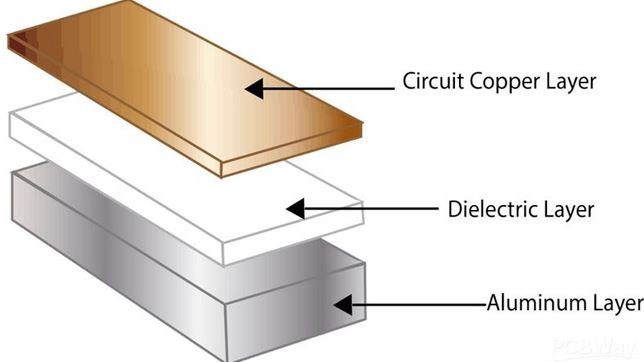
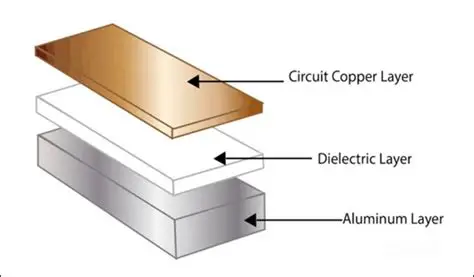
An aluminum PCB consists of a metal core, typically aluminum, bonded to a thin dielectric layer and a copper circuit layer. This construction creates a direct thermal path from heat-generating components to the metal substrate, allowing rapid heat spreading across the entire board area. In solar panel assemblies, such boards support bypass diodes, junction boxes, and monitoring electronics that must function reliably under continuous outdoor exposure. The approach aligns with established quality expectations outlined in IPC-6012E for rigid printed boards, ensuring consistent performance across production batches. Engineers select aluminum PCBs when thermal resistance must remain low without compromising electrical safety or mechanical stability.
Technical Principles of Thermal Management in Solar Panel PCBs
Heat generated by solar cells under full irradiance raises module temperature and reduces open-circuit voltage by approximately 0.3 to 0.5 percent per degree Celsius. Aluminum PCBs mitigate this effect because the metal core conducts heat laterally and vertically far more effectively than fiberglass-based laminates. The dielectric layer between the copper traces and the aluminum base is engineered to provide electrical insulation while preserving adequate thermal transfer. Proper selection of dielectric thickness and filler materials balances insulation requirements against thermal performance targets. This layered structure also helps control coefficient of thermal expansion mismatch between the board and attached components, reducing mechanical stress during daily temperature cycling.
Related Reading: The Ultimate Guide to Aluminum PCB Stackup Design: Optimizing Performance and Reliability
Practical Design and Assembly Best Practices
Designers begin by calculating expected heat load from diodes and power electronics, then determine the minimum aluminum thickness needed to keep junction temperatures within safe limits. Trace widths and copper weight are optimized to carry current without excessive voltage drop while contributing to heat spreading. During assembly, reflow profiles follow guidelines consistent with J-STD-020E to prevent moisture-related defects in the dielectric layer. Post-assembly inspection includes thermal imaging to verify uniform heat distribution across the board surface. These steps ensure the finished solar panel PCB maintains both electrical integrity and thermal efficiency throughout its service life.
Manufacturing and Quality Considerations for Renewable Energy Use
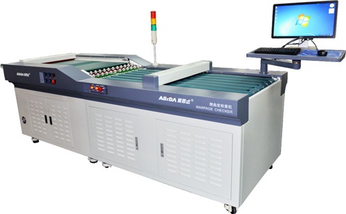
Production of aluminum PCBs for solar applications follows controlled processes that maintain dielectric uniformity and surface flatness. Warpage testing during fabrication confirms that boards remain within acceptable limits after thermal cycling, preserving contact integrity with solar cells and frames. Quality teams apply acceptance criteria from IPC-A-600K to evaluate copper adhesion, dielectric integrity, and overall board appearance. Such controls support the long-term reliability demanded by outdoor photovoltaic installations exposed to ultraviolet radiation, moisture, and temperature extremes. Consistent manufacturing practices also facilitate scalability when production volumes increase for utility-scale solar projects.
Integration Insights for Solar Module Engineers
When integrating aluminum PCBs into complete solar modules, engineers coordinate board layout with cell string design to minimize shadow effects from junction boxes. Thermal vias or direct bonding techniques further enhance heat flow from critical components into the aluminum core. System-level modeling helps predict module operating temperature under various irradiance and ambient conditions, guiding final material choices. These considerations collectively improve annual energy yield by keeping average cell temperatures lower during peak production hours.
Related Reading: Why High-Power Applications Demand Aluminum PCBs
Conclusion
Aluminum PCBs deliver measurable improvements in thermal management for solar panel assemblies, supporting higher sustained output from photovoltaic systems. Their combination of high thermal conductivity, electrical isolation, and mechanical robustness aligns well with the demanding requirements of renewable energy installations. By following established industry standards for design, fabrication, and quality verification, engineers achieve reliable performance across diverse environmental conditions. Continued refinement of dielectric materials and layout techniques will further strengthen the role of these boards in efficient solar power generation.
FAQs
Q1: How does an aluminum PCB improve thermal management in solar panels?
A1: An aluminum PCB provides a low-resistance path for heat generated by solar cells and associated electronics, keeping operating temperatures lower than those achieved with conventional substrates. This temperature reduction helps maintain higher voltage output and conversion efficiency throughout daylight hours. The approach supports long-term reliability in outdoor environments where daily thermal cycling occurs.
Q2: What role does a solar panel PCB play in efficient solar power systems?
A2: A solar panel PCB carries current from bypass diodes and monitoring circuits while dissipating heat that would otherwise reduce cell performance. Proper thermal design ensures consistent power delivery and protects sensitive components from overheating. These boards contribute directly to overall system efficiency in residential and utility-scale installations.
Q3: Why are aluminum PCB solar cells preferred for high-temperature environments?
A3: Aluminum PCB solar cells benefit from the metal core's ability to spread heat rapidly, preventing localized hotspots that degrade photovoltaic output. The construction maintains electrical isolation while providing mechanical support suitable for framed modules. This combination helps sustain performance when ambient temperatures rise during peak sunlight periods.
Q4: How does PCB design for renewable energy address long-term reliability?
A4: PCB design for renewable energy incorporates material selections and layout practices that withstand ultraviolet exposure, moisture, and repeated temperature changes. Quality verification against recognized standards confirms adhesion, dielectric strength, and dimensional stability. These measures support decades of service with minimal degradation in power generation capability.