 ALLPCB


Introduction
Differential pair routing forms a cornerstone of modern RF PCB design, enabling reliable transmission of high-frequency signals while mitigating noise and interference. In applications ranging from wireless communications to radar systems, these paired traces carry complementary signals that enhance signal quality RF through common-mode rejection. As frequencies push into the microwave regime, precise control over routing geometry becomes essential to preserve signal integrity and minimize losses. Engineers must navigate unique challenges posed by electromagnetic behavior at these speeds, where even minor asymmetries can degrade performance. This article explores the special considerations for differential RF routing, offering structured insights for optimal implementation.
What Are Differential Pairs and Why They Matter in RF Designs
Differential pairs consist of two closely spaced conductors that propagate equal and opposite signals, leveraging differential signaling to cancel out common-mode noise. This configuration proves particularly valuable in RF PCB design, where external electromagnetic interference and internal crosstalk threaten signal quality RF. By maintaining tight coupling between the traces, the pair achieves high common-mode rejection ratio, crucial for preserving the integrity of microwave differential pairs operating above 1 GHz. Industry relevance stems from their use in balanced transmission lines, mixers, and high-speed data interfaces within RF modules. Without proper routing, imbalances lead to mode conversion, increased insertion loss, and bit error rates in digital RF systems. Adhering to structured design principles ensures these pairs deliver the bandwidth and low noise figures demanded by contemporary applications.
Fundamental Technical Principles of Differential Pair Routing
The core principle governing differential pairs lies in controlled impedance, where the differential impedance—defined as twice the odd-mode impedance—must remain consistent along the entire length. In RF contexts, this requires precise trace width, spacing, and dielectric thickness to match source and load impedances, preventing reflections that distort waveforms. Edge-coupled pairs on the same layer offer simplicity but demand uniform ground plane proximity, while broadside-coupled pairs in adjacent layers provide stronger coupling at the cost of interlayer alignment. Microwave differential pair behavior introduces frequency-dependent effects like dielectric dispersion, where varying permittivity alters propagation velocity. Conductor losses from skin effect further attenuate signals, necessitating low-loss substrates. These mechanisms underscore the need for symmetric routing to avoid skew-induced common-mode noise conversion.
IPC-2221B outlines generic requirements for such controlled geometries in printed board design, emphasizing uniformity to support high-frequency performance.
Impedance Control Challenges in RF Differential Routing
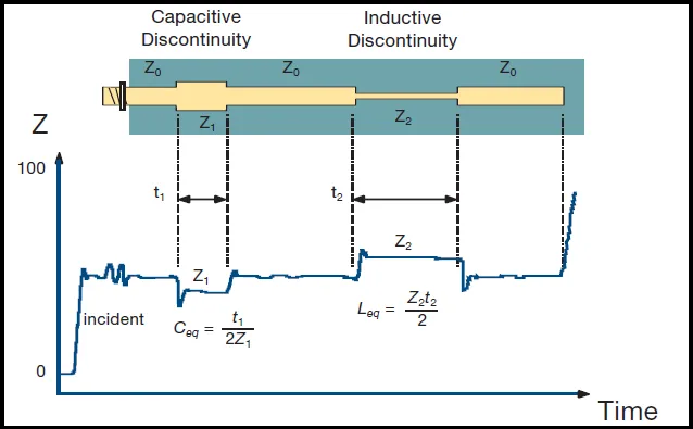
Impedance controlled RF routing demands meticulous stackup planning, as microstrip configurations expose traces to air, yielding higher effective dielectric constants than striplines. Variations in copper roughness or resin content can shift impedance by several ohms, critical at microwave frequencies where quarter-wave lengths shrink to millimeters. Engineers calculate odd-mode and even-mode impedances separately, ensuring the pair's effective differential value aligns with protocol specs. Vias introduce stubs that resonate, disrupting impedance continuity unless back-drilled or tuned. Coupling coefficient, dictated by trace separation, must balance intra-pair tightness against inter-pair crosstalk. IPC-2141A provides guidelines for these calculations, aiding designers in predicting transmission line characteristics without field solvers.
Maintaining signal quality RF involves minimizing radiation from unbalanced fields, achieved through continuous reference planes beneath the pair. Discontinuities like bends or pads cause return loss peaks, observable in S-parameter simulations.
Frequency-Specific Considerations for Microwave Differential Pairs
At microwave frequencies, wavelength shortening amplifies routing sensitivities, turning minor length mismatches into phase errors that degrade eye diagrams. Differential RF pairs must account for dispersion in laminate materials, where signal velocity varies across the spectrum, leading to pulse broadening. Conductor proximity effect concentrates current at edges, altering effective width and thus impedance. Radiation losses increase with frequency, especially in microstrip topologies lacking full ground shielding. Mode conversion from differential to common mode occurs under asymmetric coupling, exciting cavity resonances in the PCB. These principles guide routing away from high-density areas to preserve isolation.
Best Practices for Routing Differential Pairs in RF PCBs
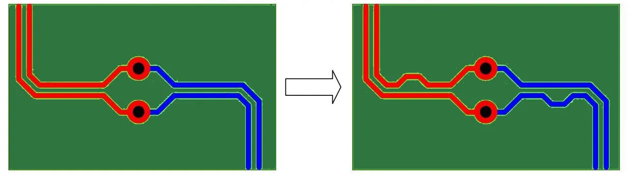
Begin with stackup definition, selecting symmetric builds with low-Dk cores for uniform fields in impedance controlled RF traces. Route pairs as unbroken serpentine or straight lines, matching lengths to within tolerances dictated by bit time, typically tighter than digital designs. Employ 45-degree bends or chamfers to reduce reflections, avoiding right angles that create capacitive discontinuities. Place vias symmetrically, pairing positive and negative signals to maintain balance, and use blind vias where possible to shorten stubs. Isolate pairs from aggressors with ground stitching vias forming fences along edges. Verify routing post-layout through time-domain reflectometry models to confirm impedance profiles.
For multilayer boards, alternate layers for orthogonal routing minimizes coupling to adjacent signals. Ground pour cutouts under pairs prevent parasitic capacitance while ensuring return path integrity.
Troubleshooting Common Issues in Differential RF Routing
Length mismatch manifests as inter-symbol interference, resolvable by meander tuning while preserving coupling. Impedance bumps from etch variations require fab feedback loops for tolerance tightening, often under 10% deviation. Crosstalk spikes indicate insufficient spacing; widen gaps or add shielding traces. Via resonances show in frequency sweeps as nulls; mitigate with radial stubs or removal. Common-mode imbalance from asymmetric bends demands mirror-image routing. Systematic post-route analysis identifies these, ensuring compliance with performance specs.
IPC-6018D specifies qualification tests for high-frequency boards, including transmission loss measurements vital for microwave differential pair validation.
Advanced Insights: Coupling and Discontinuity Mitigation
Intra-pair coupling strength, quantified by coupling factor, optimizes noise rejection but risks over-coupling at high frequencies, converting modes. Optimal spacing yields 50-70% coupling without excess. Discontinuities at transitions demand compensation, like tapered sections for pad entries. In dense RF PCB design, broadside pairs excel vertically but require via-in-pad for layer changes. Hybrid routing combines topologies for flexibility. These techniques elevate signal quality RF in complex assemblies.
Conclusion
Differential pair routing in RF designs demands precision in symmetry, impedance control, and discontinuity avoidance to uphold signal quality RF. By grasping principles like mode propagation and frequency effects, engineers craft robust microwave differential pairs resilient to real-world imperfections. Best practices—from stackup optimization to verification—align with industry standards, ensuring first-pass success. Implementing these considerations not only meets performance targets but also streamlines fabrication and testing. RF PCB design evolves with tighter margins, rewarding structured approaches for superior outcomes.
FAQs
Q1: What role does impedance control play in differential RF routing?
A1: Impedance controlled RF ensures matched transmission lines, preventing reflections that degrade signal quality RF. Per IPC-2141A guidelines, trace geometry dictates odd-mode impedance, critical for microwave differential pairs. Variations cause standing waves, increasing loss. Proper control via stackup and spacing maintains 50-ohm single-ended or 100-ohm differential targets common in RF.
Q2: How do you maintain symmetry in microwave differential pair routing?
A2: Symmetry preserves balance, avoiding common-mode conversion in differential RF signals. Route traces mirror-image, matching lengths and bends precisely. Symmetric vias and reference planes underpin this. IPC-2221B stresses uniform geometries for high-speed boards. Deviations amplify noise, harming RF PCB design integrity.
Q3: Why is length matching crucial for signal quality RF?
A3: Length matching synchronizes arrival times, minimizing skew in differential pairs. In RF PCB design, picosecond mismatches distort phases at microwave frequencies. Meander structures equalize paths without altering coupling. This upholds eye opening and BER. Standards like IPC-6018D test for such performance in high-frequency boards.
Q4: What are common pitfalls in RF differential pair via placement?
A4: Asymmetric vias disrupt impedance and balance in impedance controlled RF routing. Place pairs adjacently with equal stub lengths, preferring back-drilling. They introduce inductance, peaking return loss. Ground vias nearby aid return currents. Proper planning avoids these in microwave differential pair designs.
References
IPC-2141A — Design Guide for High-Speed Controlled Impedance Circuit Boards. IPC, 2004
IPC-2221B — Generic Standard on Printed Board Design. IPC, 2012
IPC-6018D — Qualification and Performance Specification for High Frequency (Microwave) Printed Boards. IPC, 2022


