 ALLPCB


Introduction
PCB prototyping serves as a critical phase in electronics development, where design concepts transition into physical boards for testing and validation. Incorporating Design for Manufacturability (DFM) best practices early in this process minimizes errors, accelerates iterations, and ensures reliable performance under real-world conditions. For electric engineers focused on rapid prototyping, DFM acts as a bridge between innovative designs and production feasibility, reducing costly rework and delays. By prioritizing manufacturability testing during design validation, teams can achieve faster time-to-market while maintaining high quality standards. This article explores how PCB prototyping DFM streamlines workflows through structured guidelines and factory insights.
What Is PCB Prototyping DFM and Why It Matters
PCB prototyping DFM refers to the systematic evaluation of a design's compatibility with manufacturing processes before fabrication begins. It encompasses checks for features like trace widths, via placements, and material selections that align with production capabilities. In rapid prototyping, where speed is paramount, DFM prevents issues such as etching defects or assembly failures that could extend lead times from days to weeks. Design validation through DFM ensures the prototype mirrors high-volume production outcomes, allowing engineers to identify and resolve potential flaws upfront. Manufacturability testing within DFM frameworks also optimizes costs by avoiding material waste and excessive tooling adjustments. Ultimately, adopting these practices enhances reliability, supports scalable designs, and aligns with industry expectations for robust electronics.
Key Technical Principles of DFM in PCB Prototyping
Effective PCB prototyping DFM relies on foundational principles rooted in material behavior, fabrication tolerances, and assembly constraints. Engineers must consider copper weight and foil thickness to prevent issues like over-etching during patterning, ensuring uniform conductivity across layers. Minimum trace and space dimensions, typically governed by panel size and imaging resolution, directly impact signal integrity and yield rates in multilayer boards. Via design principles, including drill sizes and aspect ratios, are crucial to avoid plating voids that compromise interlayer connections. Solder mask and silkscreen alignments further influence manufacturability by protecting traces while facilitating component placement. Adhering to these principles during design validation facilitates smooth transitions to prototyping and beyond.
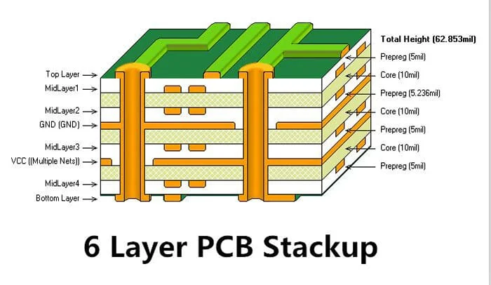
Layer stackup integrity forms another core principle, where symmetric constructions mitigate warpage from thermal expansion mismatches. Controlled impedance calculations for high-speed signals require precise dielectric thickness and material constants, integrated early to support rapid prototyping goals. Panelization strategies, such as tab routing and fiducial marks, enhance handling during fabrication and testing phases. Manufacturability testing often reveals imbalances in copper distribution, which can lead to uneven plating; balanced pours help maintain flatness. These technical elements collectively ensure prototypes withstand environmental stresses without compromising functionality.
Standards like IPC-6012E provide qualification benchmarks for rigid printed boards, emphasizing performance specs that guide DFM decisions. Compliance with such guidelines verifies that prototypes meet durability thresholds for electric applications.
Best Practices for Implementing DFM in Rapid Prototyping
Start DFM integration at the schematic capture stage by selecting materials with proven thermal and mechanical properties suited to prototyping volumes. Conduct preliminary manufacturability testing using design rule checks for clearances around pads and components, preventing shorts during reflow soldering. Optimize via farms and escape routing to distribute stress evenly, reducing delamination risks in high-density interconnects. Incorporate test points and probe zones strategically to enable thorough design validation without altering core layouts. Factory-driven insights recommend simulating panel yields based on array configurations, adjusting for v-scoring or perforations as needed.
During Gerber file generation, verify polarity and netlist integrity to eliminate open circuits common in rapid prototyping rushes. Employ annular ring allowances exceeding minimums for high-reliability vias, accommodating drill wander in standard processes. Solder joint profiles should follow J-STD-020E for moisture sensitivity, prebaking boards to avoid popcorn effects in prototypes. Perform a final DFM review with cross-functional input, focusing on assembly tolerances like component lead coplanarity. These practices streamline PCB prototyping DFM, yielding prototypes ready for immediate functional testing.
Bullet-point checklists prove invaluable for consistent application:
- Confirm trace/space rules match fabrication capabilities (e.g., 4/4 mil for high-density).
- Balance copper on each layer to minimize bow and twist below 0.75%.
- Position fiducials at least 0.1 inches from board edges for optical alignment.
- Specify surface finishes compatible with prototyping lead times, such as ENIG for fine-pitch.
Regular audits of these elements during design validation cycles reinforce manufacturability testing efficacy.
Common Challenges and Troubleshooting in Manufacturability Testing
One prevalent challenge in PCB prototyping DFM involves warpage from asymmetric stackups, often detected post-lamination. Troubleshooting entails redesigning with core materials of matching coefficients of thermal expansion, verified through flatness measurements. Bridging in fine-pitch soldering arises from inadequate stencil apertures; adjusting release angles and paste volumes resolves this during rapid prototyping trials. Voiding in vias stems from air entrapment during plating; increasing rinse cycles and agitation in process simulations mitigates it. Design validation uncovers impedance mismatches from unaccounted trace lengths; serpentine adjustments or length tuning tools correct these preemptively.
Another issue is drill breakout on inner layers, exacerbated by high aspect ratios exceeding 10:1. Reducing stack height or opting for laser drilling for blind vias addresses this in manufacturability testing. Factory insights highlight the value of iterative feedback loops, where prototype teardowns inform rule refinements. By systematically tackling these hurdles, engineers enhance prototype reliability and accelerate development timelines.
Conclusion
Streamlining PCB prototyping with DFM best practices empowers electric engineers to deliver robust, production-ready boards efficiently. From initial design validation to final manufacturability testing, these approaches minimize risks and optimize rapid prototyping workflows. Key principles like balanced stackups and precise tolerances, aligned with standards such as IPC-A-600K for board acceptability, form the backbone of success. Implementing checklists and troubleshooting protocols further bridges design intent with fabrication realities. Ultimately, prioritizing PCB prototyping DFM fosters innovation while upholding quality, positioning teams for seamless scaling to volume production.
FAQs
Q1: What is PCB prototyping DFM, and how does it support rapid prototyping?
A1: PCB prototyping DFM involves analyzing designs for manufacturing compatibility, covering aspects like trace routing and via reliability. It supports rapid prototyping by identifying issues early, reducing iteration cycles from weeks to days. Engineers perform manufacturability testing via rule checks and simulations, ensuring prototypes align with production processes. This approach cuts costs and accelerates validation for time-sensitive projects.
Q2: Why is design validation crucial in PCB prototyping DFM?
A2: Design validation in PCB prototyping DFM confirms that layouts meet fabrication tolerances before committing to prototypes. It prevents defects like insufficient annular rings or impedance drifts that plague high-speed boards. Through tools and reviews, engineers verify compliance with standards, enabling reliable rapid prototyping outcomes. This step safeguards against rework, preserving project momentum.
Q3: How can manufacturability testing improve PCB prototyping efficiency?
A3: Manufacturability testing evaluates prototype feasibility through checks on solderability, warpage, and assembly fits. It streamlines PCB prototyping DFM by flagging panelization flaws or material mismatches upfront. Factory-aligned practices, such as balanced copper distribution, boost yields and shorten lead times. Regular testing integrates seamlessly into design validation for optimal results.
Q4: What role do industry standards play in rapid prototyping DFM?
A4: Industry standards guide PCB prototyping DFM by defining acceptable limits for features like drill sizes and surface finishes. They ensure prototypes withstand thermal cycling and mechanical stresses in electric applications. Compliance facilitates design validation and manufacturability testing, promoting consistency across prototypes. Engineers reference them to align designs with proven benchmarks.


