 ALLPCB


Dielectric thickness plays a central role in antenna design, particularly when engineers seek to balance resonant behavior with overall system performance. In applications ranging from wireless communication modules to radar systems, the height of the dielectric layer directly influences how electromagnetic waves propagate and interact within the structure. Proper selection of this parameter helps achieve desired operating frequencies while maintaining acceptable levels of radiated power. Engineers routinely evaluate trade-offs between thickness, material properties, and circuit layout to meet performance targets in compact assemblies. This consideration becomes especially relevant in designs that incorporate dielectric resonator antennas, where the substrate serves both as a mechanical support and an active element in wave confinement.
What Is Dielectric Thickness in Antenna Design and Why It Matters
Dielectric thickness refers to the vertical dimension of the insulating layer placed beneath or around the radiating elements in an antenna structure. This dimension affects the effective dielectric constant experienced by the electromagnetic fields, which in turn determines the resonant frequency of the assembly. In dielectric resonator antenna configurations, the thickness contributes to the overall volume that supports the resonant modes. Industry professionals recognize that variations in this parameter can shift the frequency response antenna characteristics, sometimes by several percent, depending on the surrounding geometry. The choice of thickness also impacts antenna efficiency by influencing losses associated with surface waves and radiation resistance. When thickness is optimized, designers achieve better impedance matching and reduced power dissipation in the substrate.
Technical Principles and Mechanisms
The resonant frequency of a dielectric resonator antenna depends on the physical dimensions and the relative permittivity of the material. Increasing the dielectric thickness lowers the resonant frequency because the effective wavelength inside the medium lengthens. This relationship arises from the boundary conditions that define the allowed field distributions within the resonator volume. At the same time, thicker layers can increase the quality factor, narrowing the bandwidth unless compensated by other design adjustments such as slot coupling or feed positioning. Antenna efficiency suffers when excessive thickness promotes higher-order modes or enhances dielectric losses, converting more energy into heat rather than radiated fields. Structured analysis of these interactions follows established electromagnetic theory, where the cutoff conditions for each mode are solved from the characteristic equations involving the dielectric constant antenna value and the aspect ratios of the resonator. Engineers apply these principles during initial layout to predict how small changes in height translate into measurable shifts in return loss and radiation patterns.
Practical Solutions and Best Practices
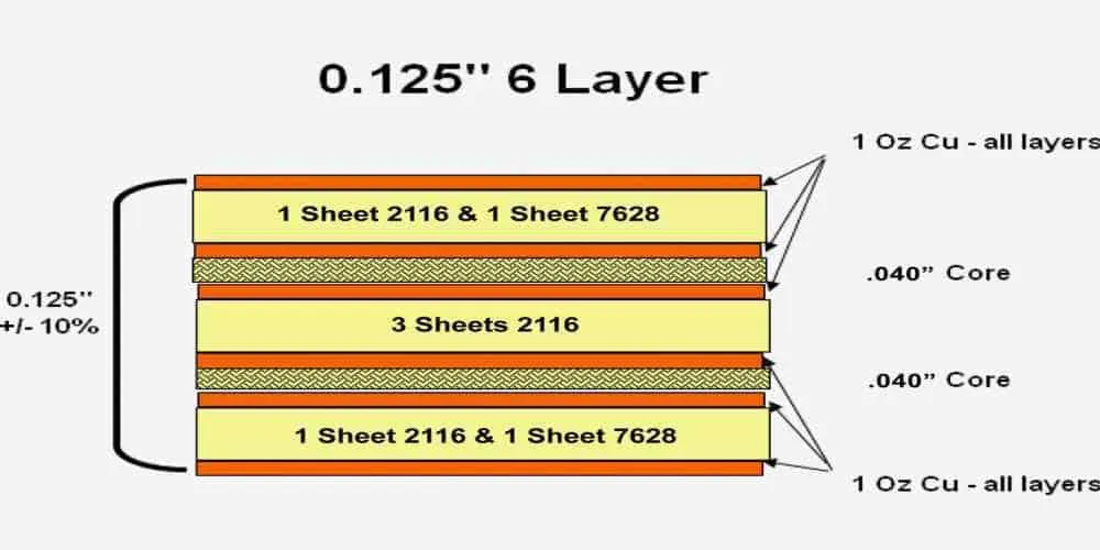
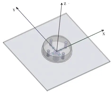
Designers begin by defining target frequency bands and then select substrate thickness that places the fundamental resonance within the required window. Simulation tools allow iterative adjustment of height while monitoring the resulting S-parameters and radiation efficiency. In practice, engineers often start with standard laminate thicknesses available from material suppliers and refine the value through parametric studies. When working with multilayer printed circuit boards, the cumulative effect of multiple dielectric layers must be considered, as the effective permittivity becomes a weighted average influenced by each layer's thickness. Compliance with IPC-6012E helps ensure that the fabricated boards maintain the specified dielectric properties and dimensional tolerances needed for repeatable antenna performance. Testing under controlled conditions verifies that the assembled unit meets efficiency targets before integration into larger systems.
Best practices also include accounting for manufacturing tolerances, because even small deviations in thickness can alter the frequency response antenna behavior. Engineers specify tighter control on core and prepreg thicknesses during board fabrication to minimize variation. When higher efficiency is required, thinner dielectrics may be chosen to reduce surface-wave losses, although this choice can raise the resonant frequency and necessitate compensatory changes in lateral dimensions. Conversely, applications that demand wider bandwidth sometimes benefit from moderately increased thickness combined with appropriate feeding techniques. Documentation of these decisions supports traceability and facilitates future revisions of the design.
Case Study Insights from PCB Design Practice
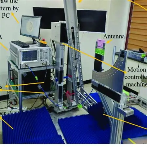
In a typical PCB design project involving a dielectric resonator antenna operating near 5 GHz, the initial substrate thickness of 1.6 mm produced a resonance slightly below the target band. Systematic reduction of the dielectric height in simulation shifted the response upward while preserving acceptable return loss. Final prototypes fabricated according to IPC-A-600K visual and dimensional criteria confirmed that the adjusted thickness delivered the required frequency alignment and maintained radiation efficiency above 70 percent across the band of interest. This outcome illustrates how controlled modification of dielectric thickness, combined with adherence to acceptance standards, enables predictable performance without extensive redesign of the conductor pattern.
Conclusion
Dielectric thickness remains a fundamental variable that engineers adjust to align resonant frequency, bandwidth, and efficiency in antenna design. Understanding the underlying electromagnetic mechanisms allows systematic optimization rather than trial-and-error approaches. When combined with rigorous adherence to fabrication standards such as those outlined in IPC-6012E, the resulting assemblies exhibit consistent behavior across production runs. Continued attention to this parameter supports the development of reliable, high-performance wireless systems that meet the demands of modern electronic equipment.
FAQs
Q1: How does dielectric thickness influence frequency response antenna performance?
A1: Dielectric thickness changes the effective electrical length of the resonator, shifting the resonant frequency higher when the layer is thinned and lower when it is thickened. This adjustment also affects bandwidth and the distribution of higher-order modes. Proper selection ensures the operating band aligns with system requirements while preserving acceptable return loss characteristics.
Q2: What role does dielectric constant antenna value play when selecting thickness for a dielectric resonator antenna?
A2: The dielectric constant determines how much the physical thickness must be adjusted to achieve a given resonant frequency. Higher permittivity materials allow smaller overall dimensions, including reduced height, for the same operating frequency. Engineers evaluate both parameters together to balance size constraints against efficiency and bandwidth targets.
Q3: Why is antenna efficiency sensitive to dielectric thickness in practical designs?
A3: Thicker dielectrics can increase dielectric losses and excite surface waves that reduce radiated power. Conversely, excessively thin layers may raise the quality factor too much, narrowing bandwidth and complicating impedance matching. Balanced thickness selection, verified through measurement, maximizes the ratio of radiated to input power.
Q4: How do industry standards guide dielectric thickness control in antenna PCBs?
A4: Standards such as IPC-A-600K define acceptability criteria for dielectric layer uniformity and thickness variation across the board. Following these guidelines during fabrication reduces performance scatter between units. Consistent application of the requirements supports reliable frequency response antenna behavior in volume production.





