 ALLPCB


Through-hole technology remains essential in many electronic assemblies where mechanical strength and high-current handling are required. Design for assembly practices help engineers create layouts that support reliable placement, soldering, and inspection of plated through-hole components. Effective DFA reduces defects during wave soldering and manual operations while maintaining consistent quality across production runs. Proper attention to lead forming, hole sizing, and component orientation prevents common issues such as solder skips, bridges, and mechanical stress on joints. These guidelines focus on practical steps that improve yield without adding unnecessary complexity to the design process.
Why DFA Guidelines for Through-Hole Components Matter
Through-hole component assembly demands careful planning because leads must pass cleanly through board holes and form strong solder fillets. Poor layout choices often lead to rework on the assembly line, increasing cost and cycle time. Wave soldering DFA becomes especially important when boards contain mixed technology with both surface-mount and through-hole parts. Component lead trimming after insertion must be considered early so that trimmed lengths meet acceptance criteria without damaging pads or traces. Manual assembly DFA applies when automated insertion equipment cannot handle certain component packages or board sizes. Following structured guidelines helps teams achieve repeatable results across prototypes and volume production.
Technical Principles of PTH Component Placement and Assembly
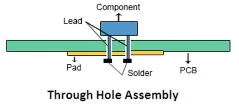
Hole diameter and pad size directly influence solder flow and joint strength during wave soldering. Leads require sufficient clearance to enter holes without forcing the board, yet the annular ring must remain large enough for reliable wetting. Component body height and lead bend radius affect how parts sit on the board and how heat transfers during soldering. Orientation of polarized parts and the direction of leads relative to the wave travel path determine whether solder reaches all joint areas evenly. Thermal mass differences between large connectors and small resistors can create uneven heating that leads to incomplete fillets or component damage. Spacing between adjacent through-hole parts must allow for clinching tools and inspection access after insertion.
Practical Best Practices for Wave Soldering DFA
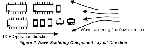
Engineers should align component rows parallel to the direction of board travel through the wave to promote consistent solder contact. Placing taller components on the trailing edge of the board helps prevent shadowing of smaller parts. Minimum lead protrusion below the board should be specified to ensure full barrel fill while avoiding excessive length that interferes with fixtures. Clinch angles and directions need standardization so that automated or manual trimming produces uniform results. Thermal relief patterns on power planes reduce heat sinking that can cause cold joints on large leads. Test points and fiducials should remain clear of component bodies to support both assembly and later inspection.
Component lead trimming guidelines call for leaving enough length for mechanical retention before soldering while trimming to final height afterward. Trimming too short before soldering risks parts falling out during handling. Trimming after soldering must avoid nicking the solder fillet or lifting pads. Clear documentation of trim lengths and acceptable variation helps operators maintain consistency across shifts.
Manual Assembly DFA and Troubleshooting Common Issues
When automated insertion is not feasible, manual placement requires adequate finger clearance around dense areas. Marking component outlines on the silkscreen layer speeds accurate placement and reduces orientation errors. Pre-forming leads to the correct bend radius before insertion prevents stress on the component body during assembly. Boards with heavy copper or thick laminates may need preheating to avoid thermal shock when large leads enter the wave. Solder bridges between closely spaced leads often result from insufficient spacing or incorrect wave parameters; increasing lead pitch or adding solder thieves can resolve this.
Insufficient barrel fill typically traces back to hole size too small for the lead or flux application problems. Open joints appear when leads are not centered or when board warpage lifts pads during soldering. Visual inspection criteria should reference clear acceptance limits for fillet shape, wetting, and lead protrusion to catch issues early.
Case Study Insight: Mixed-Technology Board Assembly
A mixed-technology board containing both fine-pitch surface-mount devices and multiple through-hole connectors experienced repeated solder skips on the connectors. Analysis showed that the connectors were placed perpendicular to the wave direction, creating large shadowed zones. Rotating the connectors ninety degrees and adding thermal reliefs on the planes improved fill rates significantly. Lead lengths were standardized before trimming, which reduced variation in joint appearance and eliminated post-solder rework for most units. These changes were implemented without altering the schematic, only through layout adjustments and updated assembly notes.
Conclusion
Applying DFA principles to through-hole components improves first-pass yield and reduces assembly cost. Attention to hole sizing, lead orientation, trimming specifications, and wave travel alignment addresses the most frequent sources of defects. Consistent documentation and reference to established acceptance criteria help maintain quality as designs move from prototype to production. Engineers who incorporate these practices early in the layout phase achieve more robust assemblies with fewer changes later in the process.
FAQs
Q1: What are the main DFA guidelines through hole engineers should follow for reliable PTH component assembly?
A1: Key practices include selecting hole diameters that allow easy lead insertion while providing adequate annular ring for soldering, orienting components to minimize shadowing during wave soldering, and specifying consistent lead protrusion and trim lengths. These steps reduce defects such as incomplete fillets and solder bridges while supporting both automated and manual assembly flows.
Q2: How does wave soldering DFA differ from surface-mount considerations for through-hole parts?
A2: Wave soldering DFA focuses on lead direction relative to wave travel, thermal relief design to prevent heat sinking, and sufficient spacing to avoid bridging between adjacent leads. Surface-mount processes emphasize pad design and stencil aperture, whereas through-hole assembly must also account for lead clinching and post-solder trimming to achieve full barrel fill and mechanical strength.
Q3: Why is component lead trimming important in manual assembly DFA?
A3: Proper trimming after insertion retains parts during handling and soldering, while final trimming after soldering produces uniform joint appearance and prevents interference with fixtures or enclosures. Inconsistent trim lengths can cause mechanical stress or inspection failures, so early specification of acceptable ranges supports repeatable manual processes.
Q4: What PTH component placement rules help prevent common soldering defects?
A4: Placing components parallel to the wave direction, maintaining minimum lead-to-lead spacing, and using thermal reliefs on copper planes promote even solder flow and full wetting. Avoiding placement of tall parts upstream of smaller ones reduces shadowing, and clear silkscreen outlines aid accurate manual insertion when automation is not used.
References
IPC-A-610G — Acceptability of Electronic Assemblies. IPC, 2017
J-STD-001H — Requirements for Soldered Electrical and Electronic Assemblies. IPC, 2020
IPC-2221B — Generic Standard on Printed Board Design. IPC, 2012


