 ALLPCB


If you’re looking for IMS PCB layout guidelines or metal core PCB design rules, you’ve come to the right place. Insulated Metal Substrate (IMS) PCBs are a powerful solution for applications requiring excellent thermal management, such as LED lighting, automotive electronics, and power supplies. Designing an IMS PCB layout for reliability involves optimizing thermal via placement in IMS PCB, careful component placement for IMS PCB, and addressing key insulated metal substrate design considerations. In this comprehensive guide, we’ll walk you through the best practices to ensure your IMS PCB design is both efficient and durable.
What is an Insulated Metal Substrate PCB?
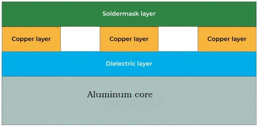
An Insulated Metal Substrate (IMS) PCB, also known as a metal core PCB, is a specialized type of circuit board designed for superior heat dissipation. Unlike traditional FR4 boards, an IMS PCB features a metal base layer—often aluminum or copper—covered by a thin dielectric layer and topped with copper circuitry. This structure allows heat to transfer away from critical components, making IMS PCBs ideal for high-power and high-heat applications.
Understanding the unique structure of IMS PCBs is the foundation for effective design. With thermal management at the core of their purpose, every layout decision must prioritize heat dissipation while maintaining electrical performance and reliability.
Why IMS PCB Layout Design Matters
A well-designed IMS PCB layout ensures efficient heat dissipation, prevents component overheating, and extends the lifespan of your electronics. Poor layout choices can lead to thermal hotspots, reduced performance, and even premature failure of components. By following proven IMS PCB layout guidelines and metal core PCB design rules, you can avoid these pitfalls and create a reliable product.
Let’s dive into the best practices for designing an IMS PCB layout, focusing on thermal management, component placement, and other critical factors.
Key IMS PCB Layout Guidelines for Reliability
Designing an IMS PCB requires a different approach compared to standard FR4 boards. Below are the essential guidelines to follow for a reliable and efficient layout.
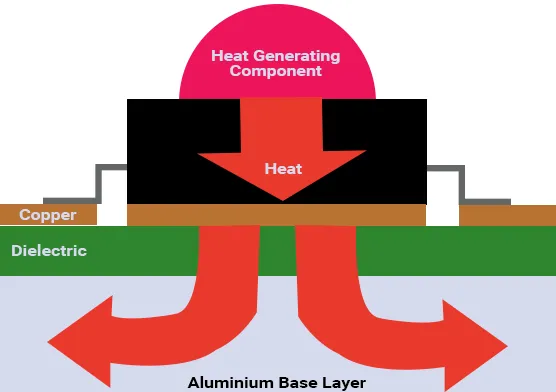
1. Prioritize Thermal Management in Your Design
The primary advantage of an IMS PCB is its ability to dissipate heat. To maximize this benefit, your layout must focus on thermal management. The metal substrate acts as a heat sink, so the goal is to transfer heat from components to the substrate as efficiently as possible.
- Minimize Thermal Resistance: Use a thin dielectric layer with high thermal conductivity. Typical dielectric thickness ranges from 20 to 100 micrometers, balancing thermal performance with electrical insulation. A thinner layer reduces thermal resistance but must maintain sufficient dielectric strength (often 500-1000V) to prevent breakdowns.
- Choose the Right Materials: Select a dielectric material with enhanced thermal conductivity, such as ceramic-filled or boron-filled prepreg. These materials can achieve thermal conductivity values of 1-3 W/mK, compared to standard prepreg at around 0.3 W/mK.
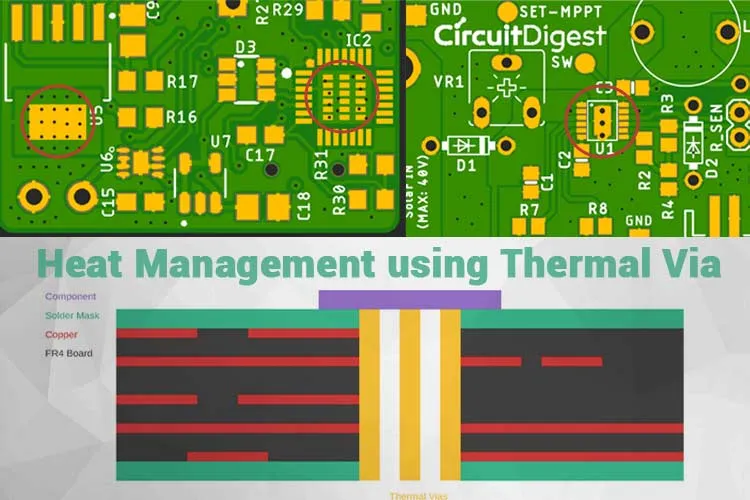
2. Optimize Thermal Via Placement in IMS PCB
Thermal vias are critical for transferring heat from the top layer of the PCB to the metal substrate. Proper thermal via placement in IMS PCB can significantly improve heat dissipation.
- Place Vias Close to Heat Sources: Position thermal vias directly under or near high-power components like power transistors or LEDs. This minimizes the distance heat must travel to reach the metal base.
- Use Multiple Vias: A single via may not be enough for high-heat components. Use an array of vias (e.g., 4-8 vias per component) to increase the thermal path. For example, a component dissipating 5W might require vias with a combined thermal resistance of less than 10°C/W.
- Via Size and Spacing: Use vias with a diameter of 0.3-0.5mm for optimal heat transfer. Space them at least 1.5 times the via diameter apart to avoid structural weakening of the board.
- Fill Vias if Possible: Filled or plugged vias improve thermal conductivity compared to open vias. Copper-filled vias can reduce thermal resistance by up to 30%.
By strategically placing thermal vias, you ensure that heat is efficiently conducted away from sensitive components, reducing the risk of overheating.
3. Focus on Component Placement for IMS PCB
Effective component placement for IMS PCB is another crucial factor in achieving reliability. Poor placement can create thermal hotspots or interfere with heat dissipation.
- Place High-Power Components Strategically: Position heat-generating components, such as power ICs or resistors, near areas with direct access to the metal substrate or thermal vias. Avoid clustering high-power components in one area to prevent localized overheating.
- Maximize Spacing: Provide adequate spacing between components to allow heat to dissipate evenly. For instance, maintain at least 2-3mm spacing between high-power components to avoid thermal interference.
- Consider Airflow: If your design includes active cooling (e.g., fans), align components to take advantage of airflow patterns. Place taller components downstream of airflow to avoid blocking cooling for smaller parts.
4. Follow Metal Core PCB Design Rules for Electrical Performance
While thermal management is the primary focus, electrical performance cannot be overlooked. Adhering to metal core PCB design rules ensures signal integrity and prevents interference.
- Ground Plane Design: Use a solid ground plane connected to the metal substrate (if feasible) to reduce electromagnetic interference (EMI). Ensure the ground plane is uninterrupted near sensitive analog or high-frequency signals.
- Trace Width and Spacing: Calculate trace widths based on current-carrying capacity and heat dissipation. For high-current traces, use wider tracks (e.g., 0.5-1mm for 5A) to minimize resistive heating. Maintain spacing of at least 0.2mm between traces to prevent crosstalk.
- Avoid Sharp Corners: Use 45-degree angles or rounded corners for traces to reduce signal reflection and stress concentration, which can impact reliability in high-frequency designs.
5. Address Insulated Metal Substrate Design Considerations
Beyond thermal and electrical factors, there are additional insulated metal substrate design considerations to keep in mind for a reliable IMS PCB layout.
- Board Thickness: The metal substrate thickness typically ranges from 0.8mm to 2mm, depending on the application. Thicker substrates (e.g., 1.6mm) provide better heat spreading for high-power designs but increase weight and cost.
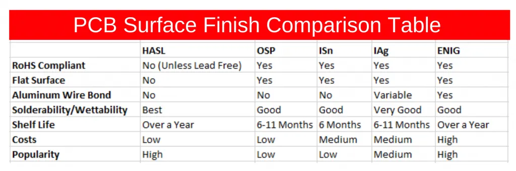
- Surface Finish: Choose a surface finish that supports both thermal and electrical performance. Electroless Nickel Immersion Gold (ENIG) is often preferred for its flat surface and corrosion resistance, unlike Hot Air Solder Leveling (HASL), which can create uneven surfaces affecting thermal contact.
- Mechanical Stability: IMS PCBs can be more rigid than FR4 boards due to the metal core. Account for this during enclosure design to avoid stress on mounting points or connectors.
Common Challenges in IMS PCB Design and How to Overcome Them
Designing for IMS PCBs comes with unique challenges. Below are some common issues and practical solutions to address them.
Balancing Thermal and Electrical Insulation
The dielectric layer in an IMS PCB must provide electrical insulation while allowing heat to pass through. If the layer is too thick, thermal resistance increases; if too thin, it risks breakdown. Work with your PCB manufacturer to select a dielectric material with a thermal conductivity of at least 1 W/mK and a dielectric strength of 500V or higher for most applications.
Managing Cost vs. Performance
High-performance materials, such as ceramic-filled dielectrics or copper substrates, can drive up costs. For cost-sensitive projects, consider using aluminum as the metal base (thermal conductivity of ~200 W/mK) instead of copper (~400 W/mK) while still achieving adequate heat dissipation for many applications.
Ensuring Manufacturability
IMS PCBs often have unique fabrication requirements due to the metal core. Avoid overly complex designs with excessive vias or fine traces that may be difficult to manufacture. Stick to standard design rules, such as minimum trace widths of 0.15mm and via diameters of 0.3mm, unless your project demands tighter tolerances.
Applications of IMS PCBs and Design Tailoring
IMS PCBs are widely used in industries where heat management is critical. Tailoring your design to the specific application can further enhance reliability.
- LED Lighting: Focus on thermal via placement under LED chips to manage heat from high brightness. Use a thicker metal base (e.g., 1.6mm) for larger fixtures dissipating over 10W.
- Automotive Electronics: Prioritize robust ground planes to handle EMI from nearby systems. Ensure components are spaced to withstand vibration and thermal cycling.
- Power Supplies: Optimize trace widths for high current (e.g., 1mm for 10A) and place power components near the board edges for better heat sinking.
Final Tips for a Reliable IMS PCB Layout
Designing an IMS PCB for reliability requires careful attention to thermal, electrical, and mechanical factors. Here are a few final tips to keep in mind:
- Simulate your design using thermal analysis software to identify potential hotspots before fabrication. Tools can predict temperature rises (e.g., a 20°C increase under load) and guide via placement.
- Collaborate with your PCB supplier early in the design process to confirm material availability and manufacturing constraints.
- Test prototypes under real-world conditions to validate thermal performance. For instance, measure junction temperatures of critical components to ensure they stay below 125°C for long-term reliability.
Conclusion
Creating a reliable IMS PCB layout is all about balancing thermal management, electrical performance, and manufacturability. By following these IMS PCB layout guidelines and metal core PCB design rules, you can optimize thermal via placement in IMS PCB, improve component placement for IMS PCB, and address critical insulated metal substrate design considerations. Whether you’re working on LED lighting, automotive systems, or power electronics, a well-designed IMS PCB can significantly enhance the performance and lifespan of your product.
At ALLPCB, we’re committed to supporting engineers with the tools and resources needed to bring innovative designs to life. With these best practices in hand, you’re ready to tackle your next IMS PCB project with confidence.


