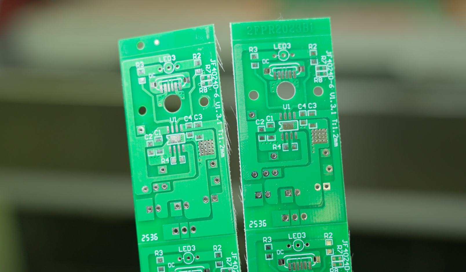
If you're diving into PCB design, you’ve likely come across the term IPC-7351. But what exactly is the IPC-7351 standard, and why is it so critical for PCB footprint dimensions, land pattern design, and SMD footprint standards? In short, IPC-7351 is a globally recognized standard that provides guidelines for creating precise land patterns for surface-mount devices (SMDs) on printed circuit boards (PCBs). It ensures your designs are reliable, manufacturable, and consistent with industry expectations. In this comprehensive guide, we’ll break down everything you need to know about IPC-7351, from its core principles to practical tips for implementation, helping you master PCB footprint design with ease.
What Is the IPC-7351 Standard?
The IPC-7351 standard, developed by the Institute of Printed Circuits (IPC), is a set of guidelines specifically created for designing land patterns for surface-mount components on PCBs. First introduced as a replacement for the older IPC-SM-782 standard, IPC-7351 has evolved through multiple revisions, with the latest being IPC-7351B, released to address modern manufacturing and assembly needs. This standard focuses on defining the optimal size, shape, and tolerances for pads, ensuring components are placed and soldered correctly during assembly.
Why does this matter? A well-designed land pattern directly impacts the reliability of solder joints, ease of assembly, and overall performance of the PCB. By adhering to IPC-7351, designers can minimize issues like tombstoning (where components lift during soldering) or misalignment, which can lead to costly rework or failures. Whether you’re working on consumer electronics, automotive systems, or industrial equipment, following this standard is a cornerstone of quality design.
Key Objectives of IPC-7351
- Standardization: Provides a universal approach to land pattern design, making it easier for manufacturers worldwide to interpret and assemble PCBs.
- Reliability: Ensures strong, consistent solder joints by defining precise pad dimensions and spacing.
- Manufacturability: Accounts for tolerances in component placement and soldering processes to reduce assembly errors.
- Scalability: Covers a wide range of component types, from tiny 0201 resistors to large QFP packages.
Why IPC-7351 Matters for PCB Footprint Dimensions
PCB footprint dimensions are the foundation of any successful design. A footprint, also known as a land pattern, includes the pads, outlines, and other features where a component will be mounted on the PCB. The IPC-7351 standard provides detailed specifications for these dimensions, ensuring that the footprint matches the component’s physical characteristics and the requirements of the assembly process.
For example, let’s consider a common SMD resistor in a 0603 package (1.6 mm x 0.8 mm). According to IPC-7351, the pad dimensions for this component might be around 0.9 mm x 0.7 mm, with a spacing of approximately 1.0 mm between pads. These measurements are not arbitrary—they account for solder fillet formation, component tolerances, and placement accuracy during automated assembly. Using these standardized dimensions prevents issues like insufficient solder or component shifting during reflow soldering.
Without adhering to IPC-7351 for PCB footprint dimensions, you risk creating designs that are difficult to manufacture or prone to defects. This standard acts as a blueprint, guiding designers to create footprints that balance functionality with production realities.
Common Footprint Dimension Categories in IPC-7351
IPC-7351 categorizes footprints based on component types and density levels. These categories help designers choose the right dimensions for their specific application:
- Most Density (M): Used for high-density designs where space is limited, often in portable electronics. Pads are smaller with tighter tolerances.
- Nominal Density (N): The standard choice for most applications, offering a balance between space and manufacturability.
- Least Density (L): Used in designs where space is not a constraint, with larger pads for easier soldering and inspection.
By selecting the appropriate density level, you can tailor your PCB footprint dimensions to match both design goals and manufacturing capabilities.
Land Pattern Design: Breaking Down the IPC-7351 Approach
Land pattern design is at the heart of IPC-7351. A land pattern includes the copper pads, solder mask openings, and other features that interface with a component on the PCB. The standard provides a systematic approach to designing these patterns, focusing on factors like pad size, shape, spacing, and orientation.
One of the key aspects of IPC-7351 in land pattern design is its emphasis on solder joint reliability. For instance, the standard recommends specific toe, heel, and side fillet dimensions for leaded components like SOICs (Small Outline Integrated Circuits). A typical SOIC-8 package might require a toe fillet of 0.5 mm to ensure proper solder flow and mechanical strength. These precise measurements reduce the risk of weak joints or thermal stress during operation.
Additionally, IPC-7351 accounts for modern assembly techniques, such as reflow soldering and pick-and-place machines. It specifies tolerances for pad placement to accommodate variations in machine accuracy, often in the range of ±0.1 mm for high-speed assembly lines. This attention to detail ensures that components are positioned correctly, even in high-volume production environments.
Steps to Implement IPC-7351 in Land Pattern Design
- Identify Component Type: Determine the package type (e.g., QFN, BGA, or chip resistor) and refer to IPC-7351 for specific guidelines.
- Select Density Level: Choose between Most, Nominal, or Least density based on your board’s space constraints and assembly process.
- Define Pad Dimensions: Use the standard’s recommendations for pad width, length, and spacing, adjusting for solder mask and paste stencil design.
- Verify Tolerances: Ensure the design accounts for manufacturing tolerances, such as ±0.05 mm for pad placement in high-density designs.
- Test and Iterate: Validate the land pattern with a prototype to confirm solder joint quality and component alignment.
Following these steps helps create land patterns that are both functional and compliant with industry norms, streamlining the transition from design to production.
SMD Footprint Standards: How IPC-7351 Ensures Consistency
Surface-mount device (SMD) footprint standards are a critical focus of IPC-7351. SMD components, such as resistors, capacitors, and ICs, dominate modern PCB designs due to their compact size and compatibility with automated assembly. However, their small dimensions and tight tolerances make precise footprint design essential.
IPC-7351 provides SMD footprint standards by defining exact pad geometries and layouts for thousands of component packages. For example, a 0402 capacitor (1.0 mm x 0.5 mm) might have pads measuring 0.6 mm x 0.5 mm with a gap of 0.4 mm between them. These dimensions ensure that the component sits flat during soldering and forms reliable electrical connections.
The standard also introduces a naming convention for SMD footprints, making it easier to identify and share designs. A footprint name like “CAPC1005X55N” indicates a chip capacitor (CAPC) with dimensions of 1.0 mm x 0.5 mm and a height of 0.55 mm under Nominal density (N). This standardized naming reduces confusion and ensures consistency across design teams and manufacturing partners.
Benefits of Following SMD Footprint Standards
- Improved Assembly Yield: Precise footprints reduce placement errors, achieving assembly yields as high as 99.9% in optimized processes.
- Reduced Design Time: Standardized footprints can be reused across projects, saving hours of manual design work.
- Enhanced Compatibility: Designs align with global manufacturing capabilities, facilitating collaboration with assembly houses worldwide.
By integrating IPC-7351 SMD footprint standards into your workflow, you lay the groundwork for high-quality, repeatable PCB production.
Practical Tips for Applying IPC-7351 in Your Designs
Implementing IPC-7351 in your PCB projects doesn’t have to be overwhelming. Here are some practical tips to help you get started and make the most of this standard:
- Use Design Software Tools: Many PCB design tools come with built-in libraries or calculators based on IPC-7351. These can automatically generate compliant footprints, saving time and reducing errors.
- Reference Official Documentation: Obtain the latest IPC-7351B documentation for detailed tables and formulas. This is especially useful for custom or less common components.
- Collaborate with Manufacturers: Share your land pattern designs with your assembly partner early in the process to confirm compatibility with their equipment and processes.
- Stay Updated: IPC standards evolve to address new technologies and challenges. Keep an eye on updates or revisions to ensure your designs remain current.
- Prototype and Test: Always validate your footprints with a small batch production run. Check for issues like solder bridging or component misalignment before full-scale manufacturing.
These actionable steps can help you seamlessly integrate IPC-7351 into your design process, leading to better outcomes for your PCB projects.
Common Challenges with IPC-7351 and How to Overcome Them
While IPC-7351 is a powerful tool, it’s not without challenges. Here are some common hurdles designers face and strategies to address them:
- Complexity of Guidelines: The standard can seem daunting due to its depth. Break it down by focusing on specific component types first, then expand your knowledge over time.
- Custom Components: Not all components have predefined footprints in IPC-7351. In such cases, use the standard’s general principles (like pad sizing formulas) to create a custom design, and verify it with testing.
- Balancing Density and Manufacturability: High-density designs (M level) can push manufacturing limits. Work closely with your production team to ensure your chosen density level is feasible with their equipment tolerances, such as ±0.05 mm placement accuracy.
By anticipating these challenges and planning ahead, you can leverage IPC-7351 effectively without compromising on design quality or production efficiency.
Conclusion: Mastering PCB Design with IPC-7351
The IPC-7351 standard is an indispensable resource for anyone involved in PCB design. By providing clear guidelines for PCB footprint dimensions, land pattern design, and SMD footprint standards, it helps ensure that your designs are reliable, manufacturable, and aligned with industry best practices. From defining precise pad sizes to offering a universal naming convention, IPC-7351 streamlines the design-to-production pipeline, saving time and reducing errors.
Whether you’re a seasoned engineer or just starting out, integrating IPC-7351 into your workflow can elevate the quality of your PCB projects. With the practical tips and insights shared in this guide, you’re well-equipped to create footprints that meet modern manufacturing demands and deliver exceptional performance. Start applying these standards today, and watch as your designs achieve new levels of precision and reliability.