 ALLPCB


Designing a printed circuit board (PCB) layout is a critical step in ensuring the functionality, reliability, and performance of electronic devices. However, many engineers, especially beginners, often fall into common traps that can lead to costly errors or performance issues. In this comprehensive guide, we’ll explore how to avoid frequent PCB layout errors by following essential PCB design guidelines. We’ll dive into key areas such as component spacing, trace routing, and signal integrity to help you create robust and efficient designs.
Whether you’re a hobbyist or a seasoned professional, understanding these principles will save you time, reduce manufacturing issues, and improve your board’s performance. Let’s break down the most common mistakes and provide actionable tips to overcome them.
Why PCB Layout Matters
A well-designed PCB layout is the foundation of a successful electronic product. A poor layout can lead to signal interference, overheating, or even complete failure of the circuit. By focusing on avoiding PCB layout errors, you ensure that your design operates as intended, meets manufacturing standards, and performs reliably under real-world conditions. Let’s look at the most common mistakes and how adhering to PCB design guidelines can prevent them.
Common PCB Layout Errors and How to Avoid Them
Even small oversights in PCB design can lead to significant problems. Below, we’ll cover the most frequent mistakes and provide practical solutions based on established PCB design guidelines.
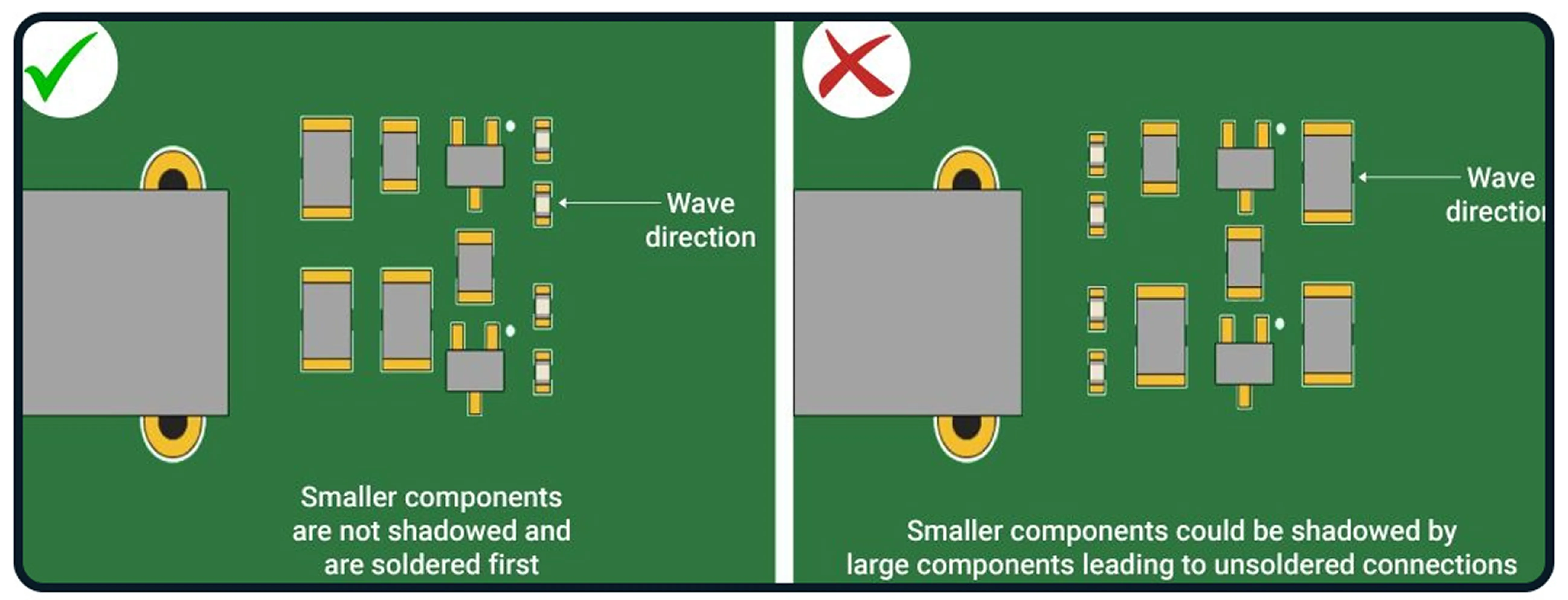
1. Incorrect Component Spacing
One of the most common PCB layout errors is improper component spacing. When components are placed too close together, it can lead to overheating, soldering difficulties, and even short circuits. On the other hand, spacing them too far apart wastes valuable board space and increases trace lengths, which can affect signal integrity.
Guideline: Follow manufacturer datasheets for minimum spacing requirements. As a general rule, maintain at least 0.5 mm (20 mils) between small components like resistors and capacitors, and 1-2 mm (40-80 mils) for larger components like ICs or connectors. For high-voltage designs, increase spacing to prevent arcing—often 3 mm or more depending on the voltage level (e.g., 3 mm for 300V).
Tip: Use design rule checks (DRC) in your PCB software to automatically flag spacing violations. This ensures components are neither too close nor unnecessarily far apart, optimizing both performance and manufacturability.
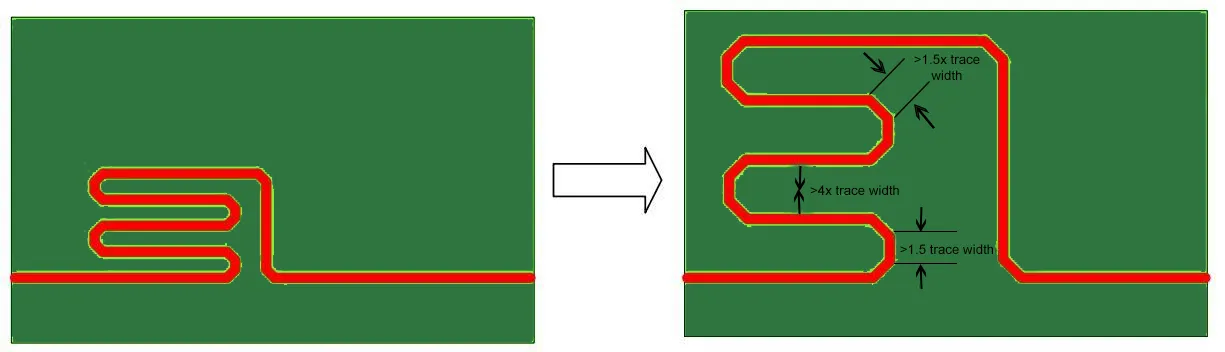
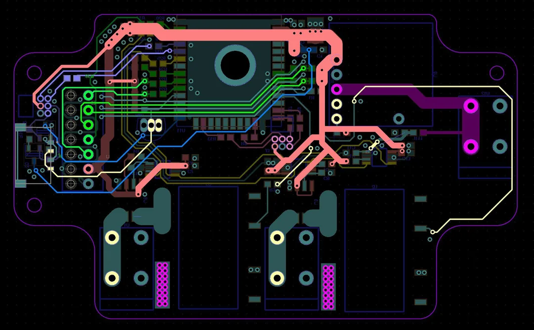
2. Poor Trace Routing Practices
Trace routing is another area where PCB layout errors frequently occur. Incorrectly routed traces can cause signal interference, increased resistance, or even complete signal failure. Common mistakes include routing traces at sharp angles, ignoring impedance requirements, or crossing high-speed signals over split ground planes.
Guideline: Always route traces at 45-degree angles instead of 90-degree corners to minimize signal reflection and electromagnetic interference (EMI). For high-speed designs, maintain consistent trace widths to control impedance—typically targeting 50 ohms for single-ended signals or 100 ohms for differential pairs. Keep trace lengths as short as possible to reduce latency and signal loss.
Tip: Separate analog and digital signals to avoid crosstalk. For example, route digital traces away from sensitive analog lines and use ground planes to shield them. If you’re working with high-frequency signals (e.g., above 100 MHz), consider using microstrip or stripline configurations to maintain signal integrity.
3. Neglecting Signal Integrity
Signal integrity is a critical factor in high-speed PCB designs, yet it’s often overlooked, leading to issues like crosstalk, EMI, or signal distortion. Poor signal integrity can cause data errors or system malfunctions, especially in designs with frequencies exceeding 50 MHz.
Guideline: To maintain signal integrity, use continuous ground planes beneath high-speed traces to provide a low-impedance return path. Avoid splitting ground planes under critical signals, as this can create noise. Match trace lengths for differential pairs to within 5 mils (0.127 mm) to prevent timing skews. Additionally, place decoupling capacitors close to power pins of ICs—within 0.1 inches (2.54 mm)—to filter out noise.
Tip: Simulate your design using signal integrity analysis tools to identify potential issues before manufacturing. For instance, if you’re designing a board with DDR4 memory running at 2400 MHz, ensure controlled impedance and minimal crosstalk by following strict routing rules for data and clock lines.
4. Inadequate Power Distribution
Power distribution problems are a frequent source of PCB layout errors. Uneven power delivery or insufficient current capacity can lead to voltage drops, overheating, or erratic behavior in components.
Guideline: Use wide traces or power planes for power distribution to minimize resistance and ensure adequate current flow. For example, a trace carrying 1A of current should be at least 20 mils (0.5 mm) wide for a 1 oz copper layer to prevent overheating. Place vias strategically to connect power planes across layers, ensuring low impedance paths.
Tip: Group components with similar power requirements together to simplify power routing. Add bulk capacitors (e.g., 10 μF) near power entry points to stabilize voltage and handle transient loads.
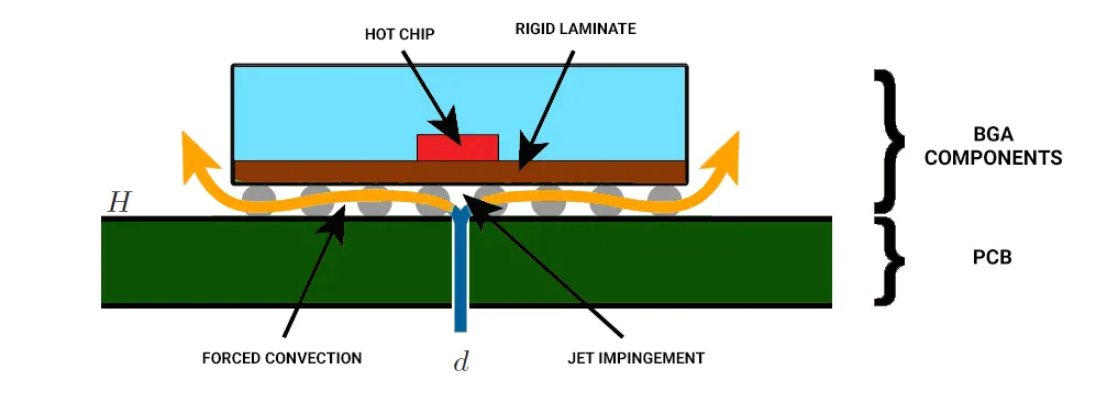
5. Ignoring Thermal Management
Heat dissipation is often underestimated in PCB design, leading to component failure or reduced lifespan. Components like power regulators or high-current ICs generate significant heat, and without proper thermal management, they can overheat.
Guideline: Place heat-generating components away from sensitive parts like sensors or low-power ICs. Use thermal vias under components like power MOSFETs to transfer heat to a ground plane or heat sink. For a component dissipating 2W of power, use at least 4-6 thermal vias with a diameter of 0.3 mm each to ensure effective heat transfer.
Tip: Incorporate copper pours or planes as heat sinks around high-power components. If possible, orient components to align with airflow in the final enclosure for better cooling.
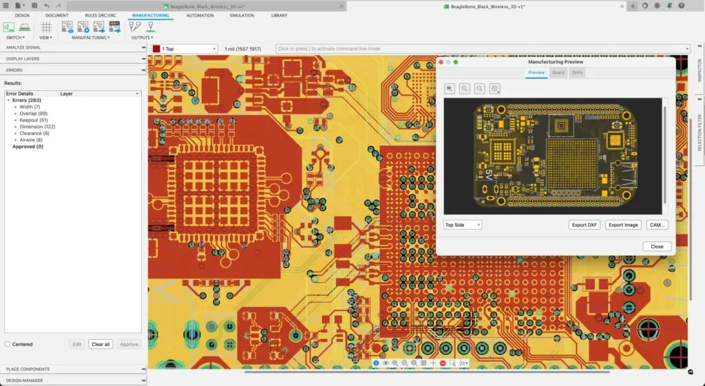
6. Overlooking Manufacturing Constraints
Many PCB layout errors stem from ignoring manufacturing limitations. Designs that don’t account for fabrication or assembly constraints can result in boards that are difficult or impossible to produce.
Guideline: Stick to standard design rules for trace widths, clearances, and drill sizes. For most manufacturers, the minimum trace width and spacing is 6 mils (0.15 mm), and the smallest via drill size is 0.3 mm. Ensure that your design fits within the board dimensions and panelization requirements to avoid extra costs.
Tip: Always generate a bill of materials (BOM) and assembly drawings to communicate clearly with the manufacturer. Double-check your footprint libraries to match the physical components, as mismatched footprints are a common source of assembly errors.
Best Practices for PCB Design Guidelines
Beyond avoiding specific mistakes, following general PCB design guidelines will elevate the quality of your layouts. Here are some best practices to integrate into your workflow for better component spacing, trace routing, and signal integrity.
Start with a Solid Schematic
A clear and accurate schematic is the blueprint for your PCB layout. Ensure that all connections are correctly defined before moving to the layout stage. This reduces the risk of routing errors or missing connections.
Use Grid-Based Placement
Align components and traces to a grid (e.g., 50 mil or 1 mm spacing) for a cleaner, more organized layout. This also makes it easier to meet spacing rules and improves the visual clarity of the design.
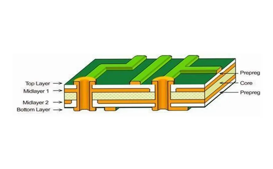
Prioritize Layer Stack-Up
For multilayer boards, plan your layer stack-up early. Dedicate specific layers to power and ground planes to minimize noise and improve signal integrity. A typical 4-layer board might use the top layer for signals, the second for ground, the third for power, and the bottom for additional signals.
Test and Iterate
Always prototype and test your design before mass production. Use simulation tools to check for signal integrity issues and thermal hotspots. Real-world testing can reveal problems that software might miss, allowing you to refine your layout.
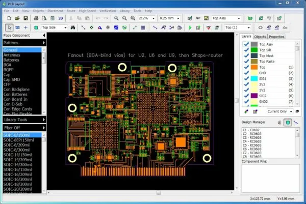
Tools and Resources for Better PCB Layouts
Modern PCB design software offers powerful features to help avoid layout errors. Use built-in design rule checks (DRC) and electrical rule checks (ERC) to catch issues early. Many tools also provide simulation capabilities for signal integrity and thermal analysis. Additionally, refer to industry standards like IPC-2221 for generic PCB design rules and guidelines.
Conclusion
Avoiding common mistakes in PCB design layout is essential for creating reliable, high-performing electronic products. By focusing on proper component spacing, effective trace routing, and maintaining signal integrity, you can prevent issues like overheating, interference, and manufacturing delays. Adhering to PCB design guidelines ensures that your boards are not only functional but also cost-effective and easy to produce.
Start by incorporating the tips and best practices discussed in this guide into your next project. With careful planning and attention to detail, you’ll minimize PCB layout errors and achieve designs that meet both performance and reliability standards. Keep learning and refining your skills, and your PCB layouts will continue to improve with each project.


