 ALLPCB


If you're diving into the world of printed circuit board (PCB) design, understanding PCB stackup is crucial. Simply put, a PCB stackup refers to the arrangement of copper layers and insulating materials in a multilayer PCB. It plays a vital role in determining signal integrity, impedance control, and overall performance of your design. Whether you're searching for a PCB stackup tutorial or tips on multilayer PCB design, this guide will walk you through the essentials of layer configuration, impedance control stackup, PCB layer arrangement, and PCB material selection to help you create efficient and reliable boards.
In this comprehensive blog, we’ll break down the concept of PCB stackup, explore its importance, and provide actionable advice for engineers and designers. Let’s get started with the fundamentals and build up to advanced considerations for optimizing your designs.
What Is a PCB Stackup and Why Does It Matter?
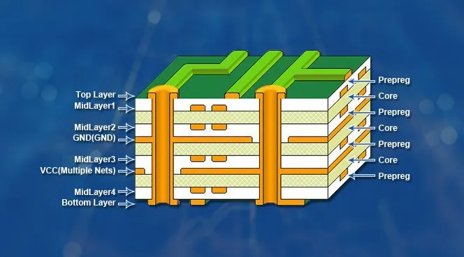
A PCB stackup is the blueprint of how layers in a multilayer PCB are organized. These layers include conductive copper layers for routing signals and power, as well as insulating layers (often called dielectric layers) that separate them. The configuration of these layers directly impacts the electrical performance, thermal management, and manufacturability of the board.
Why does this matter? A well-designed stackup can minimize issues like electromagnetic interference (EMI), crosstalk, and signal loss, especially in high-speed designs. For instance, improper layer arrangement can lead to impedance mismatches, causing signal reflections and data errors in circuits operating at frequencies above 100 MHz. On the other hand, a thoughtfully planned stackup ensures controlled impedance, better power distribution, and reduced noise, which are critical for modern electronics like smartphones, medical devices, and automotive systems.
The Basics of Multilayer PCB Design
Multilayer PCB design involves stacking multiple layers of copper and insulating materials to accommodate complex circuits in a compact space. While single-layer or double-layer boards are sufficient for simple projects, multilayer boards—ranging from 4 to 16 layers or more—are essential for advanced applications. These boards allow for denser routing, better shielding, and improved performance.
The typical structure of a multilayer PCB includes:
- Signal Layers: Used for routing high-speed signals or critical connections.
- Ground Planes: Provide a reference for signals and reduce noise by offering a low-impedance return path.
- Power Planes: Distribute power across the board, minimizing voltage drops.
- Dielectric Layers: Insulate conductive layers from each other, affecting impedance and signal speed.
For example, in a 4-layer PCB, a common stackup might be signal-ground-power-signal. This arrangement places ground and power planes in the middle to shield outer signal layers from interference. As the number of layers increases, the complexity of balancing these elements grows, making PCB layer arrangement a critical skill.
Key Elements of PCB Layer Arrangement
Arranging layers in a PCB stackup is not random; it requires careful planning to meet electrical and mechanical requirements. Here are the key factors to consider when designing your PCB layer arrangement:
1. Symmetry for Structural Integrity
A symmetrical stackup prevents warping during manufacturing. For instance, in an 8-layer board, you might arrange layers as signal-ground-signal-power-power-signal-ground-signal. This balances the copper and dielectric distribution, reducing stress during lamination and soldering processes.
2. Signal Integrity with Adjacent Ground Planes
High-speed signals should always be routed next to a ground plane to maintain a consistent return path. This minimizes loop inductance and reduces EMI. For example, at signal speeds above 1 GHz, even a small deviation in the return path can introduce noise, so placing a ground plane directly below a signal layer is a standard practice.
3. Power and Ground Plane Placement
Power and ground planes are often placed in the inner layers of the stackup to provide shielding and reduce noise. Keeping these planes close together also creates a natural capacitance, which helps filter out high-frequency noise. A typical spacing between power and ground planes might be 10 mils (0.254 mm) to achieve effective decoupling.
Impedance Control Stackup: Ensuring Signal Quality
Impedance control is a cornerstone of high-speed PCB design, and the stackup plays a pivotal role in achieving it. Controlled impedance ensures that signals travel without reflections, which can degrade performance in applications like USB, HDMI, or DDR memory interfaces.
To achieve impedance control in your stackup:
- Define Trace Geometry: The width and thickness of traces, along with their distance from reference planes, determine impedance. For a 50-ohm characteristic impedance (common in RF designs), a trace width of 6 mils on a 1.6 mm thick board with FR-4 material might be needed, depending on the dielectric constant.
- Choose Dielectric Thickness: The distance between a signal layer and its reference plane affects impedance. Thinner dielectric layers result in lower impedance, while thicker layers increase it. For instance, a dielectric thickness of 5 mils might be used for tight impedance control in high-speed designs.
- Use Simulation Tools: Software tools can calculate impedance based on stackup parameters, helping you fine-tune layer spacing and materials before fabrication.
Without proper impedance control, signal integrity suffers. For example, a mismatch in a 2.5 GHz signal path can cause up to 30% signal loss due to reflections. A well-designed impedance control stackup prevents such issues, ensuring reliable data transmission.
PCB Material Selection: Choosing the Right Foundation
The materials used in a PCB stackup significantly impact its performance, cost, and manufacturability. PCB material selection involves choosing the right dielectric and copper materials based on your design needs. Here’s what to consider:
1. Dielectric Materials
Dielectric materials insulate layers and influence signal speed and impedance. Common options include:
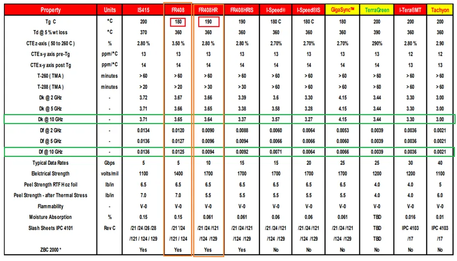
- FR-4: A standard, cost-effective material with a dielectric constant (Dk) of around 4.2-4.5. It’s suitable for most general-purpose designs but may not perform well at frequencies above 1 GHz due to signal loss.
- High-Tg FR-4: Offers better thermal stability for designs exposed to high temperatures, with a glass transition temperature (Tg) above 170°C.
- Rogers Materials: High-frequency materials with a lower Dk (around 2.2-3.0) and low loss tangent, ideal for RF and microwave applications operating at 5 GHz or higher.
2. Copper Thickness
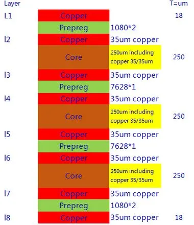
Copper thickness, measured in ounces per square foot (oz/ft2), affects current-carrying capacity and impedance. Standard options are 1 oz (35 μm) for signal layers and 2 oz (70 μm) for power planes. Thicker copper is better for high-current applications but increases cost and manufacturing complexity.
3. Thermal and Mechanical Properties
For designs in harsh environments, such as automotive or aerospace, choose materials with high thermal conductivity and mechanical strength. Some advanced materials can withstand temperatures up to 200°C without degrading, ensuring reliability in extreme conditions.
Common PCB Stackup Configurations by Layer Count
Different projects require different layer counts, and each comes with standard stackup configurations. Below are examples for common multilayer designs:
4-Layer PCB Stackup
A 4-layer board is often the simplest multilayer design, balancing cost and performance. A typical arrangement is:
- Top Layer: Signal
- Inner Layer 1: Ground
- Inner Layer 2: Power
- Bottom Layer: Signal
This setup provides shielding for signal layers and is ideal for moderate-speed designs like embedded systems.
6-Layer PCB Stackup
For more complex designs, a 6-layer stackup might look like:
- Top Layer: Signal
- Inner Layer 1: Ground
- Inner Layer 2: Signal
- Inner Layer 3: Power
- Inner Layer 4: Ground
- Bottom Layer: Signal
This adds an extra signal layer for denser routing while maintaining noise reduction with multiple ground planes.
10-Layer and Beyond
High-density designs, such as those in telecommunications or servers, often use 10 or more layers. A 10-layer stackup might include multiple signal, ground, and power layers, with careful attention to impedance control and via placement (e.g., blind and buried vias) to manage connections without overcrowding.
Best Practices for Designing a PCB Stackup
Creating an effective PCB stackup requires attention to detail and adherence to proven practices. Here are some tips to guide you:
- Collaborate Early with Manufacturers: Share your stackup design with your fabrication partner to ensure it’s manufacturable. They can advise on material availability and layer spacing tolerances, often as tight as ±10% for dielectric thickness.
- Prioritize Ground Planes: Always include at least one continuous ground plane near high-speed signal layers to stabilize impedance and reduce EMI.
- Minimize Layer Transitions: Keep high-speed signals on a single layer when possible to avoid impedance changes during via transitions, which can introduce delays of up to 100 ps in some designs.
- Test and Iterate: Use simulation tools to model your stackup for signal integrity and impedance before finalizing the design. Adjust dielectric thickness or trace widths as needed to meet specs like 50 ohms or 100 ohms for differential pairs.
Challenges in PCB Stackup Design and How to Overcome Them
Designing a PCB stackup isn’t without challenges. Common issues include:
- Cost Constraints: High-layer-count boards and advanced materials increase costs. Balance performance needs with budget by optimizing layer count—sometimes a 6-layer board can achieve what an 8-layer design would, with clever routing.
- Signal Crosstalk: Close signal layers can interfere with each other. Increase spacing or add ground planes between signal layers to reduce crosstalk, ideally keeping it below -40 dB for sensitive circuits.
- Thermal Management: High-power designs generate heat, risking delamination. Use materials with high thermal conductivity and add thermal vias to dissipate heat, targeting a thermal resistance below 1°C/W if possible.
By anticipating these challenges during the design phase, you can avoid costly redesigns and ensure a smoother transition to manufacturing.
Conclusion: Mastering PCB Stackup for Better Designs
Understanding PCB stackup is a fundamental skill for any engineer working on multilayer PCB design. From achieving impedance control to selecting the right materials, every decision in layer configuration impacts the performance and reliability of your board. Whether you’re fine-tuning a 4-layer design for a simple project or tackling a 16-layer stackup for high-speed applications, the principles of PCB layer arrangement and material selection remain the same: prioritize signal integrity, balance cost and performance, and plan meticulously.
With this PCB stackup tutorial as your guide, you’re equipped to create designs that meet modern electronics’ demands. Apply these insights to your next project, simulate your stackup for accuracy, and collaborate with manufacturing experts to bring your vision to life. A well-designed stackup isn’t just a technical necessity—it’s the foundation of innovation in circuit design.


