 ALLPCB


Designing a printed circuit board (PCB) with copper pour is a common practice to improve grounding, reduce noise, and enhance thermal management. However, improper use of copper pour can lead to issues like shorts, interference, or manufacturing defects. So, how do you ensure proper clearance and avoid shorts in your PCB layout? The key lies in following specific copper pour design rules, maintaining adequate spacing, and understanding best practices for PCB layout. In this comprehensive guide, we’ll dive deep into PCB copper pour clearance rules, preventing copper pour shorts, optimizing copper pour spacing, and essential PCB design rules for copper pour to help you create reliable and efficient designs.
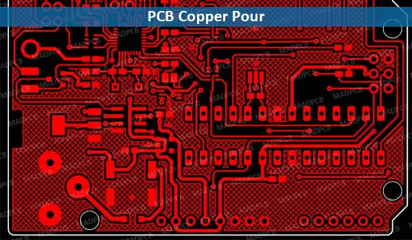
What Is Copper Pour and Why Does It Matter in PCB Design?
Copper pour, also known as copper flooding, refers to filling unused areas of a PCB layer with copper. This technique is often used to create a ground plane or power plane, which helps in reducing electromagnetic interference (EMI), improving signal integrity, and providing a low-impedance path for current. Copper pours are especially useful in high-speed designs where maintaining stable voltage levels and minimizing noise are critical.
However, without proper planning, copper pour can cause problems like electrical shorts, unintended connections, or uneven heat distribution during soldering. That’s why adhering to design rules for clearance and spacing is vital to ensure your PCB functions as intended.
Key Benefits of Using Copper Pour in PCB Layout
Before diving into the design rules, let’s explore why copper pour is a valuable tool in PCB design:
- Noise Reduction: Copper pour, especially when connected to ground, acts as a shield against EMI, reducing crosstalk between traces.
- Improved Thermal Management: Copper helps dissipate heat from components, preventing overheating in high-power circuits.
- Better Signal Integrity: A continuous copper plane provides a stable reference for high-speed signals, reducing impedance mismatches. For instance, in a 50-ohm impedance-controlled design, a ground plane can maintain signal integrity for frequencies up to 1 GHz.
- Manufacturing Efficiency: Copper pour balances the copper distribution across the board, reducing the risk of warping during fabrication.
While these benefits are significant, they can only be realized with proper implementation. Let’s explore the critical design rules to avoid common pitfalls like shorts and clearance violations.
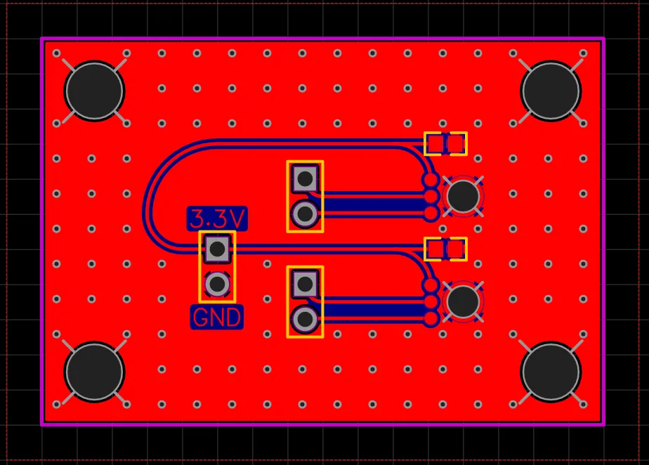
PCB Copper Pour Clearance Rules: Maintaining Safe Spacing
One of the most important aspects of copper pour design is maintaining adequate clearance between the pour and other elements on the PCB, such as traces, pads, and components. Insufficient clearance can lead to shorts or unintended connections, especially during manufacturing or soldering. Here are the essential PCB copper pour clearance rules to follow:
1. Minimum Clearance from Traces and Pads
Ensure there is enough spacing between the copper pour and signal traces or component pads to prevent accidental connections. A common guideline is to maintain a clearance of at least 8-10 mils (0.2-0.25 mm) for low-voltage designs. For high-voltage applications (above 50V), increase this clearance to 20-30 mils (0.5-0.75 mm) to avoid arcing.
2. Clearance Around Vias
Vias passing through a copper pour must have an isolation ring or clearance area to prevent shorting. A typical clearance for vias is 10-15 mils (0.25-0.38 mm) around the via barrel, ensuring no copper pour connects to it unless intended.
3. Edge Clearance from Board Outline
Keep copper pour at least 10-20 mils (0.25-0.5 mm) away from the PCB edges. This prevents copper from being exposed during board cutting, which could lead to shorts or mechanical issues during assembly.
4. Clearance for High-Speed Signals
For high-speed designs, maintain a larger clearance (15-20 mils or 0.38-0.5 mm) between copper pour and critical signal traces to avoid parasitic capacitance, which can degrade signal performance at frequencies above 100 MHz.
Avoiding Copper Pour Shorts: Best Practices
Copper pour shorts occur when the poured copper unintentionally connects to traces, pads, or other conductive elements, causing circuit failure. Here are actionable tips to prevent shorts in your PCB layout:
1. Use Thermal Reliefs for Pads
When a copper pour connects to component pads (especially for through-hole components), use thermal reliefs. These are small gaps or spoke-like connections that limit heat transfer during soldering, preventing cold solder joints while avoiding unintended shorts. A typical thermal relief spoke width is 8-10 mils (0.2-0.25 mm).
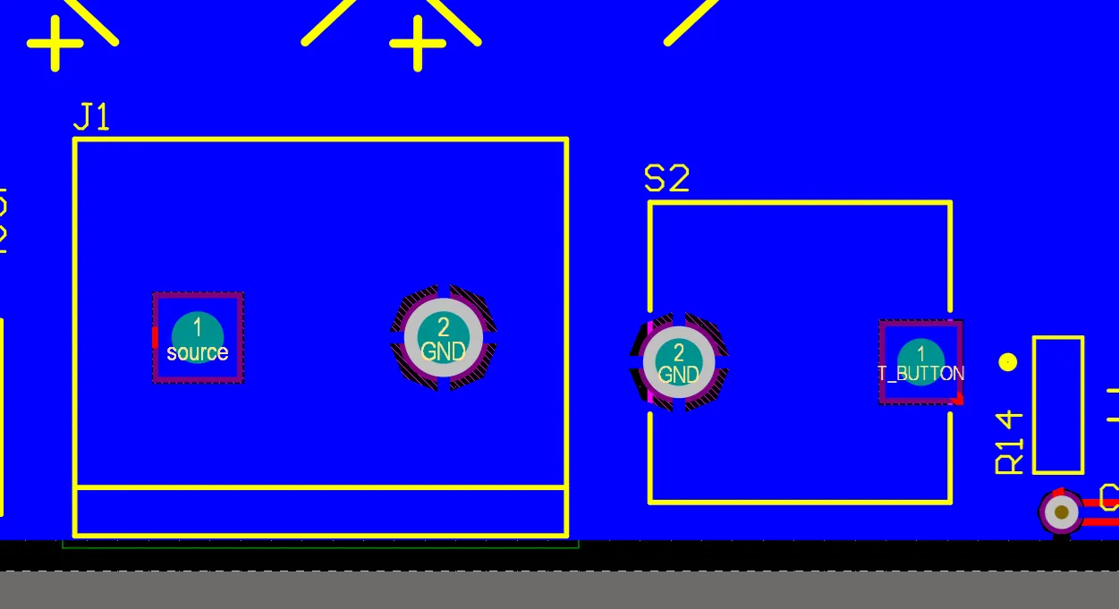
2. Implement Keep-Out Zones
Define keep-out areas in your design software to prevent copper pour from filling sensitive regions, such as under high-voltage components or near connectors. This ensures no accidental connections occur in critical areas.
3. Regularly Run Design Rule Checks (DRC)
Most PCB design tools allow you to set clearance and spacing rules. Run a DRC before finalizing your layout to identify and fix potential shorts caused by copper pour overlapping with traces or pads.
4. Avoid Overlapping Copper Pours on Adjacent Layers
In multilayer PCBs, ensure copper pours on adjacent layers do not overlap without proper insulation or clearance. Overlapping can create parasitic capacitance or shorts if vias or defects are present. Maintain at least 10-15 mils (0.25-0.38 mm) of dielectric spacing between layers.
Optimizing Copper Pour Spacing for Performance
Proper copper pour spacing not only prevents shorts but also enhances the overall performance of your PCB. Here’s how to optimize spacing for different scenarios:
1. Spacing for Ground Planes
When using copper pour as a ground plane, ensure it covers as much area as possible without violating clearance rules. For a 2-layer PCB, aim to dedicate at least 70-80% of the bottom layer to ground pour, leaving space for signal traces on the top layer.
2. Spacing for Power Planes
For power distribution, copper pour spacing should prioritize low impedance. Keep power planes close to their corresponding ground planes in multilayer designs (e.g., 5-10 mils or 0.13-0.25 mm dielectric thickness) to minimize loop inductance and improve decoupling.
3. Spacing in High-Density Designs
In high-density layouts with many components, reduce copper pour spacing to fit tight areas, but never compromise on minimum clearance (8-10 mils or 0.2-0.25 mm). Use smaller pour regions or split planes to manage density without risking shorts.
PCB Design Rules for Copper Pour: A Comprehensive Checklist
To simplify the process, here’s a checklist of PCB design rules for copper pour that every engineer should follow:
- Set minimum clearance rules (8-10 mils or 0.2-0.25 mm) for traces, pads, and vias in your design software.
- Use thermal reliefs for pads connected to copper pour to avoid soldering issues.
- Define keep-out zones around sensitive components or high-voltage areas.
- Ensure copper pour is at least 10-20 mils (0.25-0.5 mm) away from board edges.
- Connect copper pour to the appropriate net (ground or power) and avoid floating pours, which can act as antennas for EMI.
- Use via stitching to connect ground pours across layers, spacing vias at intervals of 100-200 mils (2.5-5 mm) for high-frequency designs (above 100 MHz).
- Run DRC checks to catch clearance violations or potential shorts before manufacturing.
Common Mistakes to Avoid with Copper Pour
Even experienced designers can make mistakes when implementing copper pour. Here are some pitfalls to watch out for:
- Floating Copper Pours: Unconnected copper areas can create noise or act as unintended capacitors. Always tie pours to a net like ground or power.
- Insufficient Clearance: Ignoring clearance rules can lead to shorts, especially in dense designs. Stick to the minimum spacing guidelines.
- Overuse of Copper Pour: Filling every available space without purpose can increase parasitic effects. Use pour selectively based on design needs.
- Ignoring Layer Stackup: In multilayer boards, poor planning of copper pour on adjacent layers can cause interference or capacitance issues.
Tools and Techniques for Effective Copper Pour Design
Modern PCB design software offers powerful tools to help you implement copper pour effectively. Features like automatic pour generation, clearance rule settings, and DRC checks can save time and reduce errors. Additionally, consider simulating your design for EMI and thermal performance to validate copper pour placement before manufacturing.
For complex designs, collaborate with your fabrication house to confirm their specific requirements for copper pour spacing and clearance. Some manufacturers may have stricter rules based on their equipment capabilities, such as minimum clearances of 6 mils (0.15 mm) for high-precision boards.
Conclusion: Mastering Copper Pour for Reliable PCB Layouts
Implementing copper pour in your PCB layout can significantly enhance performance by reducing noise, improving thermal management, and ensuring signal integrity. However, success depends on following strict PCB copper pour clearance rules, preventing copper pour shorts, optimizing copper pour spacing, and adhering to proven PCB design rules for copper pour. By maintaining proper clearances (8-10 mils or 0.2-0.25 mm for standard designs), using thermal reliefs, and running design rule checks, you can avoid common issues like shorts and manufacturing defects.
Whether you’re working on a simple 2-layer board or a complex multilayer design, these guidelines will help you create reliable, high-quality PCBs. Keep this checklist handy for your next project, and ensure your copper pour works for you, not against you.


