ALLPCB


Designing a printed circuit board (PCB) that transitions smoothly from schematic to assembly requires careful planning and attention to detail. One of the most effective ways to ensure success is by integrating Design for Assembly (DFA) guidelines into your workflow. DFA focuses on optimizing your design to simplify the assembly process, reduce costs, and minimize errors. In this comprehensive guide, we’ll walk you through how to incorporate DFA principles at every stage of your PCB development—from schematic review for assembly to layout considerations for DFA, BOM validation for assembly, and using a DFA checklist for design review. Whether you’re a seasoned engineer or new to PCB design, this post will provide actionable insights to streamline your process and improve manufacturing outcomes.
What Is DFA and Why Does It Matter in PCB Design?
Design for Assembly (DFA) is a set of principles aimed at making the assembly process of a product as efficient as possible. In the context of PCB design, DFA integration ensures that your board can be assembled quickly, accurately, and cost-effectively. By applying DFA guidelines, you reduce the risk of assembly errors, lower production costs, and speed up time-to-market.
Without DFA, you might face issues like misaligned components, difficult-to-solder parts, or delays due to rework. For instance, improper component placement can lead to tombstoning (where small components lift during soldering) or solder bridging (unwanted connections between pads). Studies show that assembly errors can increase production costs by up to 30% if not addressed during the design phase. By focusing on DFA integration in PCB design, you can avoid these costly mistakes.
In the sections below, we’ll explore how to embed DFA practices into each step of your PCB workflow, ensuring a seamless journey from concept to completed board.
Step 1: Schematic Review for Assembly Success
The schematic is the foundation of your PCB design, and reviewing it with assembly in mind is a critical first step in DFA integration. During this phase, you’re not just checking for electrical correctness but also ensuring that the design supports efficient assembly.
Key DFA Tips for Schematic Review:
- Standardize Components: Use standard, widely available components to avoid delays due to sourcing issues. For example, opt for resistors and capacitors with common values like 1kΩ or 10uF instead of obscure specifications.
- Minimize Component Variety: Reduce the number of unique parts to simplify inventory management during assembly. If your design uses ten different resistor values, see if you can consolidate to five or fewer.
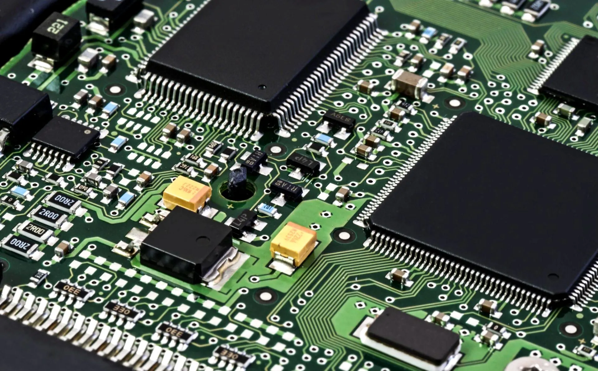
- Check for Assembly-Friendly Parts: Ensure components are suitable for automated assembly processes like surface-mount technology (SMT). Avoid through-hole components unless necessary, as they slow down assembly and increase costs.
- Label Clearly: Use clear, consistent labeling for components (e.g., R1, C2) to avoid confusion during assembly. Include polarity markings for diodes and capacitors in the schematic to prevent placement errors.
By addressing these factors during the schematic review for assembly, you set a strong foundation for the rest of the design process. A well-thought-out schematic reduces the likelihood of errors when moving to layout and assembly stages.
Step 2: Layout Considerations for DFA
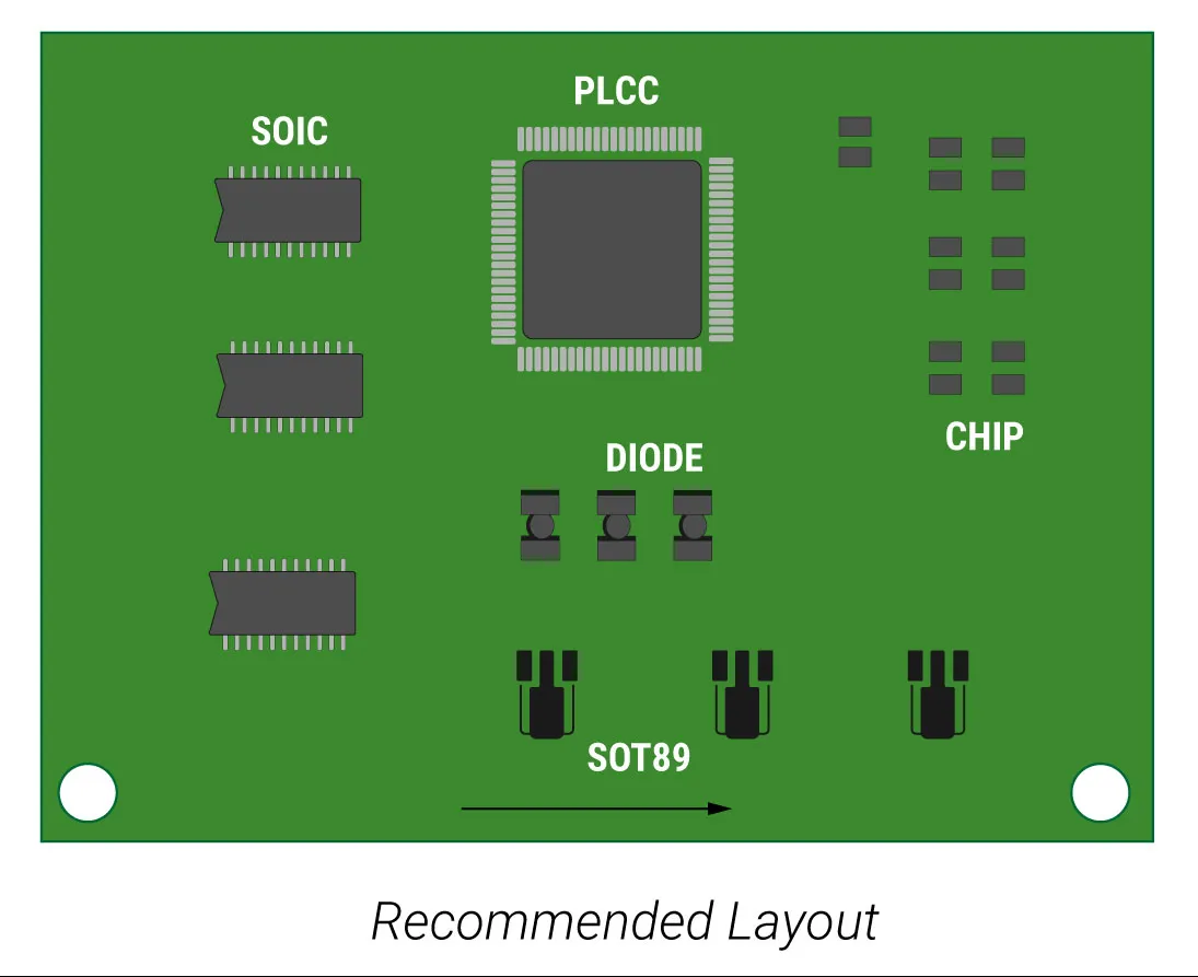
Once your schematic is finalized, the next step is creating a PCB layout that adheres to DFA principles. Layout considerations for DFA focus on component placement, spacing, and orientation to ensure the board can be assembled efficiently, whether by hand or automated machinery.
Essential DFA Layout Practices:
- Component Spacing: Leave adequate space between components to avoid interference during soldering. For SMT components, maintain a minimum spacing of 0.5mm between pads to prevent solder bridging. For larger components, increase this to 1mm or more based on manufacturer recommendations.
- Orientation Consistency: Align components in the same direction whenever possible, especially for polarized parts like diodes and LEDs. Consistent orientation reduces the risk of placement errors during automated assembly.
- Access for Soldering and Testing: Place components in a way that allows easy access for soldering tools and test probes. Avoid placing tall components near smaller ones, as they can create shadows during reflow soldering, leading to uneven heating.
- Panelization Planning: If your design will be assembled in panels (multiple boards on a single sheet), include breakaway tabs or V-scoring lines. Ensure components are at least 5mm away from panel edges to avoid damage during depanelization.
- Thermal Management: Position heat-generating components like power regulators away from sensitive parts. Include thermal vias under high-power components to dissipate heat, preventing assembly issues due to overheating.
By focusing on these layout considerations for DFA, you create a board that not only functions well but is also easy to assemble. For example, a board with poorly spaced components might require manual soldering adjustments, increasing assembly time by up to 20% compared to a DFA-optimized layout.
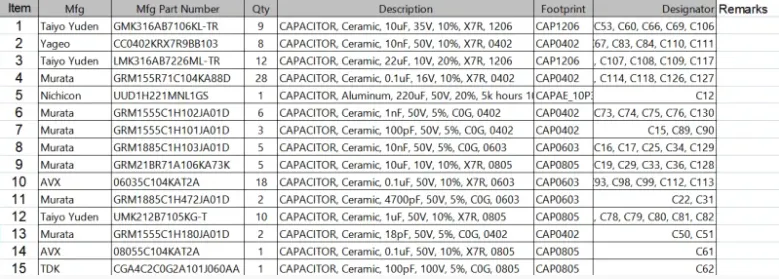
Step 3: BOM Validation for Assembly Readiness
The Bill of Materials (BOM) is a critical document that lists all components required for your PCB. BOM validation for assembly ensures that every part is correctly specified, available, and compatible with the assembly process. A poorly validated BOM can lead to delays, incorrect parts, or even complete assembly failures.
DFA-Driven BOM Validation Tips:
- Verify Part Numbers: Double-check that each component’s part number matches the manufacturer’s datasheet. Include secondary sources or alternatives in case a part is out of stock.
- Confirm Footprints: Ensure that the BOM matches the footprints used in your layout. A mismatch, such as a 0805 resistor listed for a 0603 footprint, can halt assembly.
- Check for End-of-Life (EOL) Parts: Avoid using components that are discontinued or nearing EOL. Using obsolete parts can lead to last-minute redesigns, costing time and money.
- Include Assembly Notes: Add specific instructions in the BOM for components requiring special handling, such as moisture-sensitive devices that need baking before assembly.
- Consolidate Components: As with the schematic, minimize the variety of components. For instance, if two capacitors of slightly different values (e.g., 9.8uF and 10uF) can be replaced with a single 10uF part, update the BOM accordingly.
A validated BOM is a cornerstone of DFA integration in PCB design. It ensures that the assembly team has everything they need to build your board without unnecessary delays. In fact, BOM errors are a leading cause of production delays, with some studies estimating they account for up to 15% of manufacturing setbacks.
Step 4: Using a DFA Checklist for Design Review
Before sending your design to manufacturing, conducting a thorough design review with a DFA checklist is essential. A DFA checklist for design review acts as a final safety net, catching potential issues that could complicate assembly or increase costs.
Comprehensive DFA Checklist for PCB Design Review:
- Component Placement: Are components spaced adequately (e.g., 0.5mm minimum for SMT) and oriented consistently?
- Solder Mask and Silkscreen: Is the solder mask clear of pads, and are silkscreen markings legible for assembly guidance?
- Footprint Accuracy: Do all footprints match the components listed in the BOM?
- Testing Accessibility: Are test points accessible for in-circuit testing after assembly?
- Panelization: If using panels, are breakaway tabs or scoring lines included, with components at least 5mm from edges?
- Thermal Considerations: Are heat-generating components positioned appropriately, with thermal vias if needed?
- Assembly Compatibility: Are all components suitable for the intended assembly method (SMT or through-hole)?
- BOM Validation: Is the BOM accurate, with no EOL parts or footprint mismatches?
- Documentation: Are assembly drawings, pick-and-place files, and other documentation complete and clear?
Using this DFA checklist for design review ensures that no detail is overlooked. It’s a proactive way to catch issues before they reach the assembly line, where fixes can cost significantly more. For example, correcting a footprint error during assembly might require manual rework, adding hours to the process, whereas identifying it during review takes minutes.
Benefits of Integrating DFA Guidelines in Your Workflow
Integrating DFA guidelines into your PCB workflow offers numerous advantages that go beyond just simplifying assembly. Here are some key benefits backed by industry insights:
- Cost Reduction: DFA can lower assembly costs by up to 25% by minimizing errors and reducing the need for manual intervention.
- Faster Turnaround: A DFA-optimized design can reduce assembly time by 15-20%, accelerating your product’s time-to-market.
- Improved Quality: Fewer assembly errors mean higher reliability. For instance, proper component spacing can reduce soldering defects by as much as 30%.
- Scalability: DFA prepares your design for high-volume production, ensuring that automated assembly processes run smoothly even at scale.
By embedding DFA principles at every stage—from schematic to assembly—you create a design that’s not only functional but also efficient to produce. This holistic approach saves time, money, and resources while delivering a high-quality end product.
Common DFA Mistakes to Avoid
Even with the best intentions, it’s easy to overlook certain aspects of DFA. Here are some common pitfalls and how to avoid them:
- Ignoring Component Spacing: Tight spacing might save board space but can lead to soldering issues. Always adhere to minimum spacing guidelines like 0.5mm for SMT pads.
- Using Non-Standard Parts: Unique or hard-to-source components can delay assembly. Stick to standard parts unless absolutely necessary.
- Skipping BOM Validation: An unvalidated BOM can cause major setbacks. Always cross-check part numbers and availability.
- Neglecting Test Points: Without accessible test points, post-assembly testing becomes difficult, increasing the risk of undetected defects.
Avoiding these mistakes ensures that your DFA integration in PCB design is effective and that your board moves seamlessly through assembly.
Conclusion: Streamline Your PCB Workflow with DFA
Integrating DFA guidelines into your PCB workflow is a game-changer for engineers looking to optimize their designs for assembly. By focusing on schematic review for assembly, layout considerations for DFA, BOM validation for assembly, and using a DFA checklist for design review, you can significantly reduce errors, cut costs, and speed up production. Each step of the process builds on the last, creating a cohesive strategy that ensures your board is not only functional but also easy to assemble.
Start implementing these DFA practices in your next project to experience the benefits firsthand. With careful planning and attention to detail, you’ll transform your workflow from schematic to assembly, delivering high-quality PCBs that meet both design and manufacturing goals.