 ALLPCB


Introduction
A robust power distribution network forms the backbone of reliable operation in complex electronic systems built on multilayer boards. In a 10-layer PCB, the PDN must deliver stable voltage and current to every active component while suppressing noise that could degrade signal integrity. Engineers face increasing challenges as clock speeds rise and power demands grow, requiring careful attention to plane design, capacitor selection, and overall stackup configuration. Effective 10-layer PCB PDN design directly influences thermal performance, electromagnetic compatibility, and long-term product reliability. This article examines the principles and practices that support power integrity in 10-layer PCBs, with particular emphasis on decoupling capacitors for 10-layer PCBs.
Why Robust PDN Design Matters in 10-Layer PCBs
Power integrity issues in multilayer boards often manifest as voltage droop, ground bounce, or excessive ripple that can cause logic errors or component failure. A 10-layer construction provides additional routing layers and opportunities for dedicated power and ground planes, yet it also introduces complexities in via placement and return current paths. Proper PDN planning reduces the risk of simultaneous switching noise and improves overall system efficiency. Industry standards such as IPC-2221 guide the general requirements for printed board design, ensuring that power distribution meets mechanical and electrical performance criteria. Without attention to these factors, even well-routed signal paths may suffer from intermittent faults traceable to inadequate power delivery.
Technical Principles of Power Integrity in 10-Layer PCBs
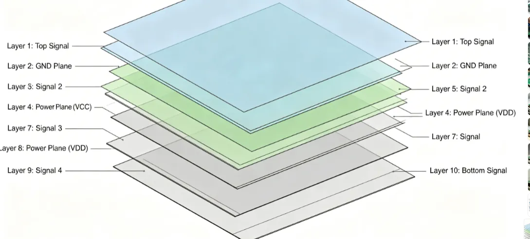
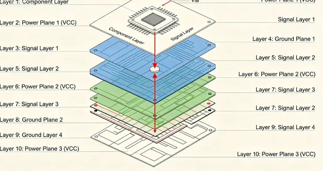
The PDN consists of power and ground planes, vias, traces, and discrete decoupling components that collectively maintain target voltage levels across the board. In a typical 10-layer stackup, inner layers are often assigned to power and ground to maximize plane capacitance and minimize inductance. Plane capacitance arises from the parallel-plate effect between adjacent copper layers separated by dielectric material, providing a distributed low-impedance path for high-frequency currents. Engineers analyze target impedance across frequency bands to determine acceptable voltage ripple, typically expressed as a percentage of nominal supply voltage. Return current paths must remain continuous to avoid creating large loop areas that radiate electromagnetic interference. These mechanisms interact closely with the board stackup, where dielectric thickness and copper weight directly affect both DC resistance and AC impedance characteristics.
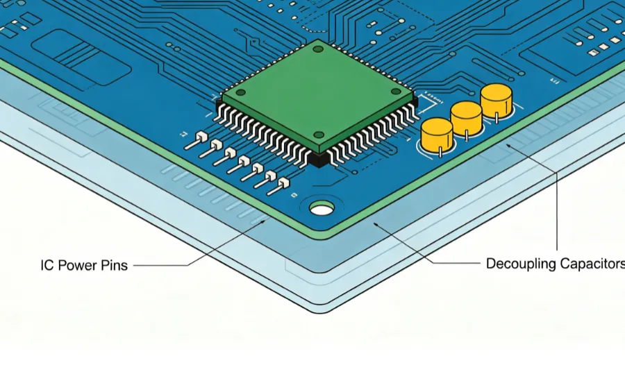
Decoupling capacitors serve as local energy reservoirs that supply transient current demands before the main power source can respond. Their effectiveness depends on equivalent series inductance, equivalent series resistance, and mounting inductance introduced by vias and pads. In 10-layer PCBs, multiple capacitor values are often placed in parallel to cover a broad frequency spectrum, with smaller values addressing higher frequencies and larger values supporting lower-frequency transients. Placement proximity to power pins reduces loop inductance and improves high-frequency performance. Simulation tools model the combined impedance profile of planes and capacitors to verify that the network stays below the target impedance curve across the operating bandwidth.
Practical Solutions and Best Practices for 10-Layer PCB PDN Design
Begin the design process by defining power requirements for each voltage rail, including maximum current, voltage tolerance, and transient response needs. Assign dedicated power and ground planes in the stackup to create low-inductance paths, typically placing them adjacent to each other to enhance interplane capacitance. Use multiple vias in parallel for power connections to reduce inductance and improve current-carrying capacity. Select decoupling capacitors based on their self-resonant frequency and combine them strategically across the board, positioning the smallest values closest to integrated circuit power pins.
Maintain continuous ground planes beneath power planes to provide well-defined return paths and minimize crosstalk. Avoid splitting planes unnecessarily, as splits can force return currents to take longer routes and increase noise. When splits are required, bridge them with stitching capacitors or vias to maintain continuity at high frequencies. Perform frequency-domain analysis to confirm that the combined impedance of planes and capacitors remains below target levels up to several hundred megahertz. Thermal considerations also influence PDN layout, as high-current paths generate heat that must be managed through copper weight and thermal vias.
Best Practices for Decoupling Capacitors in 10-Layer PCBs
Effective use of decoupling capacitors for 10-layer PCBs requires attention to both component selection and physical implementation. Choose capacitors with low equivalent series inductance and mount them using short, wide traces or direct via connections to the planes. Distribute capacitors evenly across the board rather than clustering them in one area, ensuring that every high-speed device has local bypassing. Combine bulk capacitors for low-frequency energy storage with smaller ceramic capacitors for high-frequency noise suppression. Verify the overall network through post-layout simulation that includes via inductance and plane spreading effects.
Regular review of the PDN during the design cycle helps identify potential issues before fabrication. Adjust capacitor values or add additional devices if impedance peaks exceed targets. Document the rationale for each design choice to support future revisions or troubleshooting.
Conclusion
A well-designed PDN in a 10-layer PCB ensures stable power delivery, reduces noise, and supports reliable operation of complex electronic assemblies. Attention to stackup configuration, plane continuity, and strategic capacitor placement forms the foundation of effective power integrity in 10-layer PCBs. Engineers who apply these principles achieve better electromagnetic compatibility and thermal performance while meeting the demands of modern high-speed designs. Consistent application of industry guidelines helps maintain quality across projects.
FAQs
Q1: How does stackup configuration affect 10-layer PCB PDN design?
A1: The arrangement of power and ground planes within a 10-layer stackup determines interplane capacitance and inductance, directly influencing voltage stability and noise suppression. Adjacent power-ground pairs provide distributed capacitance that supports high-frequency current demands. Proper assignment of these planes also affects return current paths and overall electromagnetic performance.
Q2: What role do decoupling capacitors play in power integrity for 10-layer PCBs?
A2: Decoupling capacitors supply transient currents locally, preventing voltage droop during rapid load changes. In 10-layer PCBs, a combination of capacitor values placed near integrated circuits covers a wide frequency range and keeps network impedance low. Their mounting inductance and proximity to power pins determine effectiveness at higher frequencies.
Q3: Why is target impedance analysis important in 10-layer PCB PDN design?
A3: Target impedance analysis identifies frequency bands where the PDN may exceed acceptable ripple limits, guiding capacitor selection and plane design. Maintaining impedance below the target curve across the operating spectrum ensures that voltage remains within tolerance under dynamic loads. This analysis integrates plane characteristics with discrete component behavior.
Q4: How can engineers improve return current paths in multilayer PDN layouts?
A4: Engineers improve return paths by keeping ground planes continuous and placing power planes adjacent to them to minimize loop area. Multiple vias in parallel for power connections reduce inductance and support higher currents. Avoiding unnecessary plane splits prevents current crowding and associated noise.
References
- IPC-2221 — Generic Standard on Printed Board Design. IPC.
- IPC-6012E — Qualification and Performance Specification for Rigid Printed Boards. IPC, 2017.


