 ALLPCB


Introduction
Immersion silver stands out as a popular lead-free surface finish for printed circuit boards, valued for its excellent solderability and uniform thin layer directly on copper. Electrical engineers often encounter immersion silver myths that question its practicality in modern designs, from tarnishing fears to doubts about long-term performance. These misconceptions stem from early experiences with inconsistent processes, but advancements in plating chemistry and handling protocols have addressed many concerns. This article separates immersion silver truth from fiction, drawing on established engineering principles and industry standards to provide clarity. By examining technical realities, engineers can make informed decisions for applications ranging from consumer electronics to telecommunications. Understanding these points ensures optimal PCB reliability without unnecessary trade-offs.
What Is Immersion Silver and Why Does It Matter?
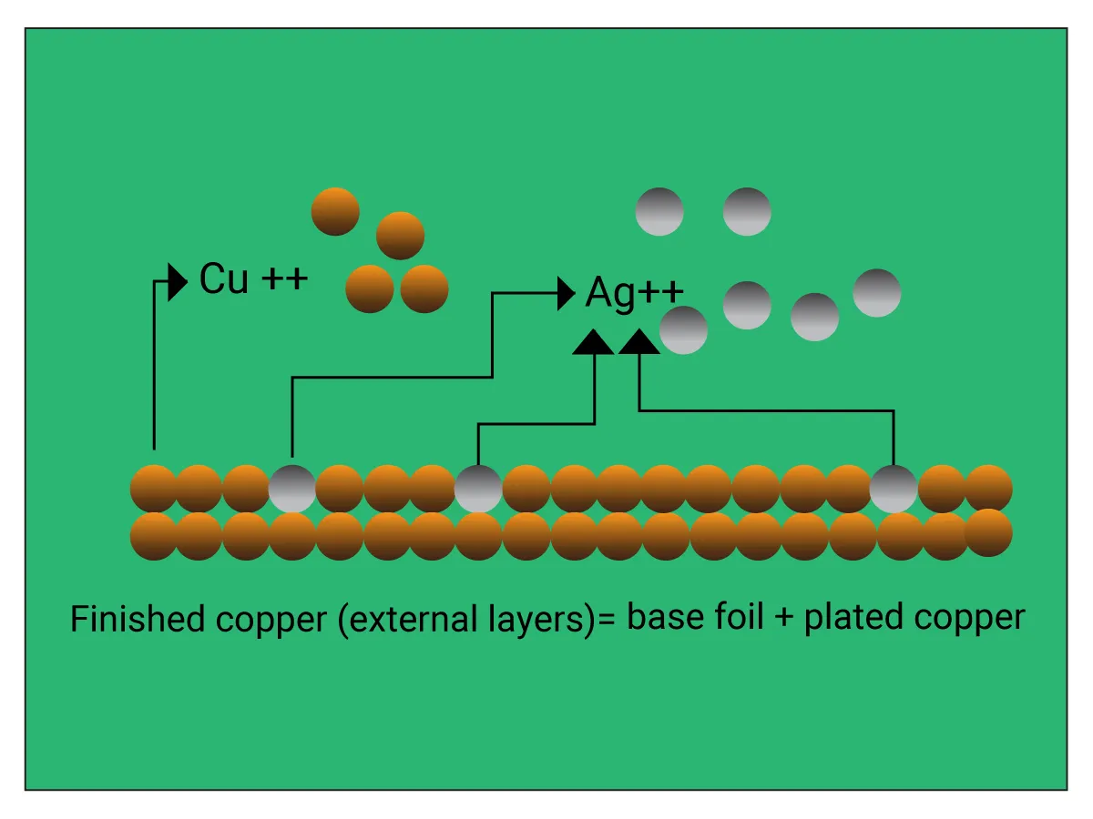
Immersion silver involves a chemical displacement process where silver ions replace copper atoms on PCB pads and traces, forming a thin, pore-free layer typically between 0.12 and 0.4 micrometers thick. This finish preserves the copper's natural flatness, unlike leaded alternatives, making it ideal for high-density interconnects and fine-pitch components. Its high electrical conductivity and low signal loss suit RF and high-speed designs, while RoHS compliance aligns with global environmental regulations. Engineers select immersion silver for its balance of performance and process simplicity in manufacturing flows. As demand grows for lead-free assemblies, its relevance increases, especially where solder joint integrity is paramount. However, persistent immersion silver myths can deter adoption despite proven capabilities.
The Technical Principles Behind Immersion Silver Performance
The immersion process relies on a redox reaction where silver deposits selectively on exposed copper, creating a metallurgical bond without electrolytic equipment. This results in a uniform coating resistant to initial oxidation, promoting consistent wetting during soldering. Silver's ductility minimizes stress in thermal cycles, reducing risks like cracking in multilayer boards. Key to its mechanism is the absence of an intermediate barrier layer, which enhances contact resistance but requires environmental controls to prevent diffusion issues. Standards like IPC-4553 outline qualification tests for thickness, solderability, and porosity, ensuring repeatability across fabricators. These principles underpin its reliability when specifications are met precisely.
In practice, the finish excels in reflow soldering due to silver's affinity for tin-based alloys, forming intermetallics that strengthen joints without excessive growth. Electrical engineers appreciate its low profile for press-fit connectors and aluminum wire bonding in power modules. However, exposure to sulfur or halides can initiate superficial tarnish, a non-destructive layer that reflow removes effectively. Proper bath chemistry controls organic inhibitors to suppress electromigration pathways under bias. This structured approach counters many perceived weaknesses, aligning with qualification under IPC-6012 for rigid boards.
Myth 1: Immersion Silver Tarnishes Quickly and Ruins Solderability
One of the most prevalent immersion silver myths claims that the finish tarnishes rapidly in air, rendering boards unsolderable after brief exposure. In reality, tarnish forms as a thin silver sulfide layer from atmospheric sulfur, but it is cosmetic and evaporates during reflow soldering without impacting joint quality. IPC-4553 specifies testing protocols that confirm solderability persists even after accelerated aging, provided initial plating meets thickness and purity requirements. Engineers report successful assembly post-storage when boards remain in controlled environments below 30 degrees Celsius and 40 percent relative humidity. Handling with gloves prevents contamination from skin oils, further extending usability. This myth persists from outdated processes lacking modern anti-tarnish additives.
Field data shows that properly packaged boards maintain performance through multiple reflow cycles, debunking the notion of inherent fragility. Tarnish sensitivity is manageable, similar to other finishes requiring care, and does not equate to reliability failure. Visual inspections per IPC-A-600 reveal no correlation between light discoloration and wetting defects. For high-volume production, this translates to consistent yields without rework.
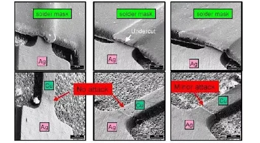
Myth 2: Immersion Silver Lacks Reliability Due to Electromigration and Creep Corrosion
Concerns about immersion silver reliability often center on electromigration and creep corrosion under humidity and voltage stress, suggesting it fails prematurely in harsh conditions. While silver can migrate dendritically in uncontrolled high-humidity scenarios, plating baths with organic suppressors per IPC-4553 minimize this risk, achieving stability comparable to alternatives in most assemblies. Creep corrosion, observed in sulfur-rich environments, affects exposed areas but is mitigated by conformal coatings or solder mask over bare silver. Qualification tests simulate operating life, showing no failures in typical telecom or automotive boards outside extreme Class 3 applications. Engineers designing for standard reliability find it outperforms thicker finishes in signal integrity due to lower inductance.
Long-term studies confirm that with bias humidity testing, modern immersion silver withstands 85 percent RH at 85 degrees Celsius without shorts. The key lies in non-solder mask defined pads to avoid mask adhesion issues that exacerbate corrosion. This addresses immersion silver limitations claims, positioning it as viable for mid-to-high reliability needs. Fabrication controls ensure void-free deposits, further bolstering joint endurance.
Myth 3: Immersion Silver Is Prohibitively Expensive
A common misconception in immersion silver cost discussions portrays it as overly pricey compared to HASL or OSP, deterring budget-conscious projects. In truth, its pricing sits moderately between basic organic finishes and premium ENIG, driven by silver's market value but offset by simpler processing without nickel plating steps. Economies of scale in high-volume runs reduce per-board costs, making it competitive for mid-tier production. Engineers balance this with superior flatness that cuts assembly defects, yielding net savings. Cost analyses show it undercuts ENIG by 20 to 30 percent while matching performance in solderability.
Material efficiency stems from thin deposition, minimizing waste, and compatibility with standard lines avoids capital upgrades. For prototypes, the premium over HASL is negligible given lead-free mandates. This immersion silver truth reveals it as a pragmatic choice without luxury pricing.
Myth 4: Immersion Silver Has Limitations with Fine-Pitch and HDI Designs
Skeptics argue immersion silver limitations prevent its use in fine-pitch or HDI boards, citing coplanarity issues or poor wetting. Conversely, its sub-micrometer profile delivers the flattest surface among common finishes, ideal for 0.3 mm pitch BGAs and laser-drilled vias. Uniform coverage ensures reliable stencil release and paste deposition, reducing bridging risks. In HDI stacks, low roughness preserves impedance control for gigabit signals. Solder joint analysis shows stronger intermetallics than matte tin, enhancing fatigue resistance.
This capability stems from conformal deposition that follows copper topography precisely. Engineers leverage it for RF modules where nickel's magnetic losses disqualify ENIG.
Best Practices for Maximizing Immersion Silver Performance
To counter immersion silver myths, adopt factory-driven protocols starting with supplier qualification to IPC-4553 thickness specs. Store boards in nitrogen-purged bags with desiccants, targeting use within six months for optimal results. During assembly, sequence reflow promptly after unpackaging and employ no-clean fluxes compatible with silver. Post-solder inspections focus on fillet wetting rather than cosmetic appearance. For exposed areas, apply edge bonds or potting to shield from pollutants.
Incoming inspections verify solderability via edge dip tests, ensuring batch consistency. Process controls like bath monitoring prevent porosity, aligning with IPC-6012 performance classes. These steps deliver immersion silver reliability in production.
Conclusion
Immersion silver emerges as a robust, cost-effective finish when myths are dispelled by engineering facts and standards adherence. From debunking tarnish fears to affirming fine-pitch prowess, its strengths in solderability and conductivity shine through proper implementation. Electrical engineers benefit from its balance in lead-free designs, avoiding over-specification pitfalls. Prioritizing handling and qualification unlocks reliable performance across applications. Embrace the immersion silver truth for efficient, high-yield PCB fabrication.
FAQs
Q1: What are the most common immersion silver myths?
A1: Immersion silver myths often include rapid tarnishing, high costs, and poor reliability in humid environments. In practice, tarnish is superficial and reflow-removable, costs are moderate versus ENIG, and electromigration is controlled via IPC-4553-compliant plating. Proper storage extends shelf life to 6-12 months, making it suitable for most assemblies. Engineers should focus on handling protocols for optimal results.
Q2: Is immersion silver reliable for electrical engineering applications?
A2: Yes, immersion silver reliability holds in telecom, automotive, and consumer boards with flat surfaces and strong solder joints. It resists thermal stress better than OSP due to metallurgical stability, though not ideal for downtime-critical Class 3 per IPC guidelines. Testing confirms endurance under bias humidity when suppressors are used. Select it confidently for mid-reliability needs.
Q3: How does immersion silver cost compare to other finishes?
A3: Immersion silver cost positions it affordably between OSP and ENIG, leveraging simple chemistry for volume savings. It avoids nickel's expense while matching solder performance, reducing assembly defects. Fine-pitch benefits offset any premium over HASL. Budget engineers find it economical for lead-free production.
Q4: What are the real limitations of immersion silver?
A4: Immersion silver limitations involve environmental sensitivity requiring sealed storage and gloves, plus avoidance in sulfur-heavy atmospheres. It excels in fine-pitch but needs coatings for bare silver exposure. Shelf life reaches 12 months properly managed, per standards. These are mitigable, not prohibitive.
References
IPC-4553 — Specification for Immersion Silver Plating for Printed Boards. IPC.
IPC-6012E — Qualification and Performance Specification for Rigid Printed Boards. IPC, 2018.
IPC-A-600K — Acceptability of Printed Boards. IPC, 2020.


