 ALLPCB


Introduction
Precision PCB drilling forms the foundation of reliable interconnects in modern printed circuit boards, enabling the placement of components and vias essential for high-density designs. As electrical engineers push for smaller form factors and finer pitches, achieving pcb drill tolerance and pcb drill accuracy becomes critical to prevent assembly failures and signal integrity issues. The pcb drilling process must balance minimum drill size specification with manufacturability constraints, where even minor deviations can lead to plating inconsistencies or mechanical stress. Controlling drill size in pcb manufacturing involves precise control over equipment parameters and material interactions. This article explores the technical principles behind accurate drilling, factory best practices, and strategies to meet stringent requirements aligned with industry standards.
Understanding the PCB Drilling Process
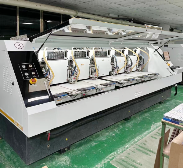
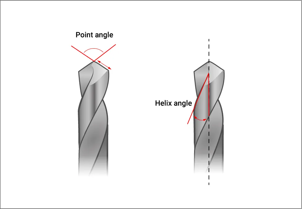
The pcb drilling process typically begins with mechanical drilling using carbide-tipped bits rotated at high speeds to create through-holes, blind vias, or microvias in copper-clad laminates. Panels are stacked with entry and backup materials to minimize burrs and delamination, while multiple peck cycles evacuate chips and reduce heat buildup. For smaller features, laser drilling employs UV or CO2 lasers to ablate material with sub-micron precision, ideal for high aspect ratios beyond mechanical limits. Drill size selection starts from the finished hole diameter, accounting for plating buildup that reduces the effective size by 0.025 to 0.075 mm per side. Factory setups optimize spindle runout below 0.005 mm and feed rates tailored to board thickness for consistent results. This process directly influences pcb drill accuracy, where deviations accumulate from bit entry to exit.
Factors Influencing PCB Drill Tolerance and Accuracy
Pcb drill tolerance defines the allowable variation in finished hole diameter, typically ranging from ±0.075 mm for standard plated through-holes under IPC-6012 guidelines. Key factors include drill wander, caused by bit deflection in fibrous glass-reinforced materials, which worsens with aspect ratios exceeding 10:1. Bit wear accelerates during high-volume production, enlarging holes progressively unless compensated by secondary drilling or bit changes. Board warpage introduces positional errors, amplifying diameter inconsistencies across panels. Environmental controls like temperature and humidity affect laminate stability, while plating chemistry variations alter final dimensions. Achieving tight pcb drill accuracy requires monitoring these variables through in-process metrology, such as automated optical inspection post-drill.
Thermal expansion during drilling generates localized heat, potentially causing resin smear that must be removed via desmear processes to maintain tolerance. Material stack-up, including copper foil thickness and prepreg types, impacts thrust forces and hole quality. For minimum drill size specification, mechanical limits hover around 0.15 mm due to bit rigidity, while laser enables 0.05 mm or smaller without mechanical stress.
Minimum Drill Size Specification in PCB Manufacturing
Minimum drill size specification depends on the hole type, board class, and fabrication class, with IPC-2221 providing design guidelines for viable aspect ratios. For plated through-holes, finished sizes below 0.20 mm challenge mechanical drilling due to chip evacuation issues, often necessitating laser alternatives. Factory capabilities dictate feasibility, where drill-to-copper spacing must exceed 0.10 mm to avoid breakout. Engineers specify drill sizes oversized by plating allowance, ensuring annular rings meet class requirements. High-density interconnects demand microvias with 0.075 mm minimums, verified post-plating. Balancing this with cost involves selecting drill charts standardized across suppliers for reproducibility.
Controlling drill size in pcb manufacturing starts at the design stage, where Gerber files include exact bit sizes and hit counts. Production panels undergo x-ray verification for layer alignment before drilling, preventing cumulative errors.
Strategies for Controlling Drill Size in PCB Manufacturing
Effective control begins with precise tooling: drill bits ground to ±0.01 mm diameter tolerance, loaded via automatic loaders to minimize handling errors. Spindle speeds of 150,000 to 200,000 RPM paired with optimized feed rates, typically 0.05 to 0.15 m/min, reduce wander in small diameters. Peck drilling with 0.1 to 0.3 mm depths clears debris, preventing bit binding that enlarges holes. Entry films with aluminum or polyester stabilize initial penetration, while backup boards absorb exit burrs. Real-time monitoring via force sensors adjusts parameters dynamically for consistent pcb drill tolerance.
Post-drill etching and plating processes must account for copper deposition uniformity, often 18 to 35 μm, which shrinks holes predictably. Factories implement statistical process control, tracking hole sizes via automated CMM or laser gauging against ±0.05 mm targets for premium boards. Material selection, like low-Dk resins, minimizes hygroscopic swelling that affects accuracy.
Best Practices for Achieving Precision in PCB Drilling
Adopt IPC-A-600 acceptability criteria early in design to set realistic pcb drill accuracy expectations across classes 2 and 3. Specify finished hole sizes rather than drill diameters in fab drawings, allowing manufacturers to adjust for plating. Limit aspect ratios to 8:1 for mechanical drills under 0.25 mm to maintain tolerance. Use panel fiducials for registration, ensuring drill positioning within ±0.075 mm. For high-volume runs, segment drills by size to extend bit life and uniformity.
Incorporate secondary operations like re-drilling oversized holes or plasma cleaning for residue-free walls. Collaborate with fabricators on drill charts compliant with IPC standards, verifying capabilities for minimum drill size specification. Simulate thermal-mechanical stresses in design tools to predict warpage impacts on drilling.
Routine maintenance of drilling machines, including collet calibration and vacuum extraction, sustains long-term accuracy. Transition to HDI stacks leverages laser for sub-0.10 mm features, hybrid with mechanical for larger vias.
Troubleshooting Common Drilling Challenges
Drill breakout at inner layers often stems from inadequate thrust control or dull bits, resolved by increasing peck frequency. Oversized holes indicate excessive wear; implement bit life counters tied to panel counts. Tapered holes result from asymmetric forces, mitigated by symmetric stack-ups and balanced tooling. Factory insights reveal that humidity above 60% exacerbates resin smear, necessitating enclosed environments. Post-plating metrology confirms compliance, rejecting panels outside tolerance.
Conclusion
Precision PCB drilling hinges on mastering pcb drill tolerance, pcb drill accuracy, and the pcb drilling process to meet evolving demands for denser boards. Controlling drill size in pcb manufacturing through optimized parameters, standards adherence, and vigilant process control ensures reliable minimum drill size specification. Electrical engineers benefit from factory-driven practices like peck drilling, real-time monitoring, and material synergies to achieve superior results. By integrating these strategies, designs transition seamlessly from prototype to production, upholding performance and yield.
FAQs
Q1: What is the typical PCB drill tolerance for plated through-holes?
A1: Pcb drill tolerance for plated through-holes is generally ±0.075 mm (±3 mils) for diameters up to 0.8 mm, as aligned with IPC-6012 standards. This accounts for drill wander, bit wear, and plating buildup. Tighter tolerances like ±0.05 mm require advanced controls and increase costs. Engineers should specify based on class and verify via post-process gauging for consistent results.
Q2: How does the PCB drilling process affect minimum drill size specification?
A2: The pcb drilling process determines minimum drill size specification through mechanical or laser methods, with mechanical limited to about 0.15 mm due to bit stability. Peck cycles and entry materials control accuracy in small holes. Laser excels for microvias under 0.10 mm, enabling HDI. Aspect ratio and plating must align with design rules for manufacturability.
Q3: What factors impact PCB drill accuracy in manufacturing?
A3: Pcb drill accuracy suffers from drill wander, bit deflection, and thermal effects during the pcb drilling process. Board warpage and material inconsistencies amplify errors. Optimizing spindle speed, feed rates, and chip evacuation maintains tolerances. Standards like IPC-A-600 guide acceptability, ensuring reliable hole quality across production runs.
Q4: How to improve controlling drill size in PCB manufacturing?
A4: Controlling drill size in pcb manufacturing involves precise bit sizing, automated loading, and statistical monitoring. Peck drilling evacuates chips to prevent enlargement, while x-ray alignment ensures positioning. Adhering to IPC guidelines for tolerances prevents over-specification. Factories use force feedback for dynamic adjustments, boosting yield on fine-pitch designs.
References
IPC-6012E — Qualification and Performance Specification for Rigid Printed Boards. IPC, 2017
IPC-A-600K — Acceptability of Printed Boards. IPC, 2020
IPC-2221B — Generic Standard on Printed Board Design. IPC, 2012


