 ALLPCB


Telecommunication base stations require printed circuit boards that handle high-frequency signals, manage substantial thermal loads, and maintain long-term reliability in outdoor environments. Engineers and procurement teams face constant pressure to control PCB manufacturing cost while meeting performance specifications. Effective approaches focus on design choices, material selection, and process optimization rather than compromising on essential quality attributes. These strategies help organizations achieve competitive pricing without sacrificing the durability demanded by network infrastructure applications.
Why Cost Management Matters in Base Station PCB Projects
Base station PCB assembly involves complex multilayer constructions that support radio frequency circuits, power distribution, and control logic. Rising component densities and stricter signal integrity requirements increase fabrication complexity, which directly influences overall project budgets. Procurement teams evaluate low-cost PCB options that still satisfy operational demands over multi-year service intervals. Successful cost control begins with early collaboration between design and manufacturing teams to identify opportunities for simplification.
Industry standards guide these decisions by establishing clear acceptance criteria. IPC-6012E defines qualification and performance requirements for rigid printed boards, helping teams align specifications with achievable manufacturing outcomes. When applied consistently, such frameworks reduce the risk of costly redesigns or field failures.
Technical Principles Behind Cost-Effective Fabrication
PCB fabrication techniques influence both unit price and long-term performance. Panelization strategies that maximize substrate utilization lower material waste and reduce per-board processing expenses. Controlled impedance routing and optimized via placement minimize the need for specialized equipment while preserving signal quality. Thermal management features, such as strategic copper distribution and heat-spreader integration, address the high power dissipation typical in base station environments without requiring exotic materials.
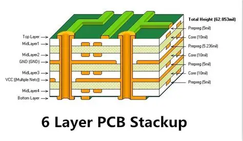
Material selection plays a central role in balancing performance and expense. Standard FR-4 variants with appropriate glass transition temperatures often suffice for many digital and mixed-signal sections, while selective use of low-loss laminates is reserved for critical RF paths. This hybrid approach avoids blanket application of premium substrates across the entire board. Stack-up design that consolidates power and ground planes further reduces layer count where electrically feasible.
Process controls during fabrication help maintain quality at lower cost. Automated optical inspection combined with targeted electrical testing catches defects early, limiting scrap rates. Warpage management through balanced copper distribution and proper curing cycles prevents assembly issues downstream. These measures align with IPC-A-600K guidelines for acceptability of printed boards, ensuring consistent output without excessive inspection overhead.
Practical Solutions and Best Practices
Design for manufacturability reviews conducted before prototyping identify opportunities to simplify layouts and reduce unique part numbers. Standardized via sizes and drill patterns allow fabricators to use common tooling, which shortens lead times and lowers setup charges. Early involvement of assembly partners during the layout phase helps optimize component placement for efficient surface-mount processes.
PCB prototyping serves as a critical checkpoint for validating cost assumptions. Multiple prototype iterations using representative materials and finishes reveal potential issues before volume production begins. This step supports informed decisions on panel configurations and surface finishes that meet both performance and budget targets. Low-cost PCB strategies often incorporate selective gold plating only on high-wear connector areas rather than full-board immersion finishes.
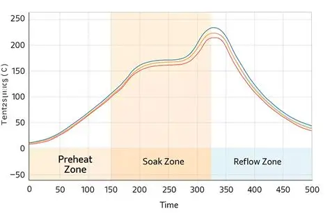
During base station PCB assembly, solder paste volume control and reflow profile optimization reduce defects such as bridging or insufficient joints. Stencil design that accounts for component pitch variations improves yield without additional process steps. Post-assembly testing focused on functional verification rather than exhaustive parametric checks further streamlines production while maintaining reliability.
Conclusion
Cost-effective manufacturing of telecommunication base station PCBs relies on disciplined application of design principles, material choices, and process controls. Early planning, adherence to recognized standards, and iterative prototyping enable teams to achieve favorable PCB manufacturing cost outcomes while preserving the quality required for network infrastructure. These methods support scalable production that meets both technical specifications and commercial objectives.
FAQs
Q1: How can PCB manufacturing cost be reduced for base station applications without affecting reliability?
A1: Early design reviews that emphasize panelization efficiency, standardized via sizes, and selective use of premium materials help lower PCB manufacturing cost. Collaboration with fabrication partners during layout ensures processes remain aligned with IPC-6012E requirements, minimizing scrap and rework while maintaining performance.
Q2: What role does PCB prototyping play in controlling expenses for base station PCB assembly?
A2: PCB prototyping validates stack-up choices, thermal performance, and assembly yields before committing to volume runs. Multiple low-volume builds identify cost drivers such as excessive layer counts or specialized finishes, allowing adjustments that support economical base station PCB assembly at scale.
Q3: Which PCB fabrication techniques most effectively balance quality and price in high-frequency designs?
A3: Techniques such as optimized copper balancing, hybrid material stack-ups, and efficient panel utilization reduce material waste and processing steps. These approaches maintain signal integrity and thermal performance while directly addressing low-cost PCB targets for telecommunication equipment.
Q4: How do industry standards influence cost decisions in base station PCB projects?
A4: Standards such as IPC-A-600K provide objective acceptance criteria that prevent over-specification and unnecessary inspection. Consistent application across design and production teams reduces variability, supports predictable yields, and helps control overall project costs without compromising board quality.
References
IPC-6012E — Qualification and Performance Specification for Rigid Printed Boards. IPC, 2017
IPC-A-600K — Acceptability of Printed Boards. IPC, 2020
J-STD-001G — Requirements for Soldered Electrical and Electronic Assemblies. IPC, 2017


