 ALLPCB


Introduction
Electronics hobbyists often start with breadboard prototypes, but transitioning to a custom PCB unlocks greater performance and reliability, especially for high-speed circuit PCB projects. In this practical electronics project, we will design, build, and test a simple signal generator paired with an amplifier circuit on a DIY PCB. This project operates at frequencies up to several megahertz, introducing key concepts like signal integrity without overwhelming complexity. By following structured steps, you will gain hands-on experience with PCB design software, soldering techniques, and circuit testing. The result is a compact device capable of generating clean square waves and amplifying them for applications like testing other circuits or driving speakers. Let’s dive into this rewarding high-speed circuit PCB project step by step.
What Is a High-Speed Circuit and Why It Matters for Hobbyists
A high-speed circuit involves signals propagating at frequencies where the wavelength approaches the physical dimensions of traces on the PCB, typically above 1 MHz for hobbyist projects. At these speeds, issues like reflections, crosstalk, and noise become prominent if not addressed in the design. Building such a circuit on a PCB teaches essential principles that scale to more advanced electronics projects, such as data acquisition or RF experimentation. Unlike low-frequency designs, high-speed layouts demand controlled impedance and minimal parasitic effects to maintain signal quality. For DIY enthusiasts, this project matters because it bridges basic prototyping with professional practices, enhancing skills in PCB design software and fabrication. Mastering these fundamentals prepares you for real-world challenges in signal generators and amplifier circuits.
Key Technical Principles Behind High-Speed PCB Design
High-speed signals behave like transmission lines when trace lengths exceed one-tenth of the signal wavelength, leading to impedance mismatches that cause ringing or attenuation. To mitigate this, maintain consistent trace widths based on stackup and dielectric properties, as outlined in IPC-2221C for generic printed board design. Ground planes provide a low-inductance return path, reducing electromagnetic interference and stabilizing voltage references essential for the amplifier circuit. Decoupling capacitors placed close to IC power pins filter high-frequency noise, ensuring clean operation of the signal generator stage. Vias introduce discontinuities, so minimize their use or stub them appropriately to preserve signal integrity. These principles form the foundation of any successful high-speed circuit PCB project.
Crosstalk occurs when adjacent traces couple magnetically or capacitively, distorting waveforms in dense layouts. Proper spacing, calculated from IPC-2221C guidelines, and routing perpendicular on different layers help isolate signals. For hobbyists, understanding rise times is crucial; faster edges demand tighter control to avoid overshoot. Thermal management also plays a role, as amplifiers generate heat that can shift component characteristics at high speeds. By applying these mechanisms logically, your DIY PCB will deliver reliable performance.
Practical Steps to Design and Build Your DIY PCB
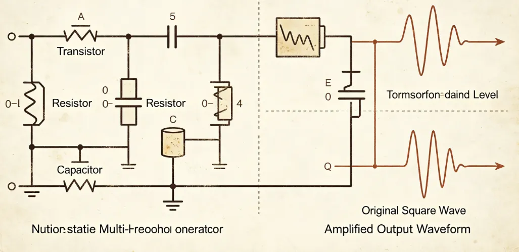
Start with the schematic in PCB design software: create an astable multivibrator signal generator using a timer IC configured for square waves around 1-5 MHz, followed by a non-inverting op-amp amplifier stage with gain adjustable via resistors. Select components like resistors for frequency setting (use formulas for R and C values), a crystal or RC network for stability, and bypass capacitors. Export the netlist and begin PCB layout on a two-layer board, prioritizing short traces for high-speed paths. Assign the signal generator output to a 50-ohm controlled impedance trace, routing it away from power lines. Fill unused areas with ground pours connected via multiple vias for shielding.
In PCB design software, set design rules for minimum trace width (e.g., 0.2 mm for signals), clearance (0.25 mm), and via sizes to match hobbyist fabrication capabilities. Place the amplifier close to the input to minimize interconnect lengths, and add test points for probing. Generate Gerber files and drill files, then send to a fab house for production. Upon receiving the bare DIY PCB, inspect for defects like shorts or opens visually, aligning with IPC-A-600M acceptability criteria. This structured approach ensures your high-speed circuit PCB project is manufacturable and functional.
Related Reading: DIY Engine Control Unit PCB: A Hobbyist's Guide to Building Your Own
Soldering and Assembly Best Practices
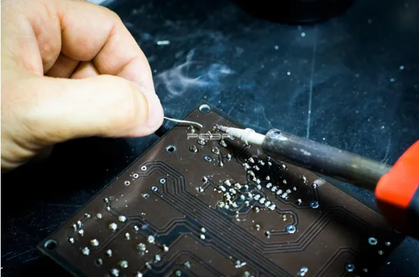
Soldering the DIY PCB requires precision to avoid cold joints or bridges, particularly on fine-pitch components in the amplifier circuit. Preheat the board to prevent warpage, apply flux, and use a temperature-controlled iron at 300-350°C for lead-free solder. Follow IPC J-STD-001J requirements for soldered assemblies, ensuring fillet shapes meet Class 2 criteria for hobbyist reliability. Start with low-profile parts like resistors and capacitors, then place the timer IC and op-amp, reflowing with hot air if needed. After assembly, clean flux residues with isopropyl alcohol to prevent corrosion. Proper technique guarantees the signal generator operates without intermittent faults.
Related Reading: How to Reflow Solder SMD Components Using a Toaster Oven: A DIY Guide
Circuit Testing and Troubleshooting Common Issues
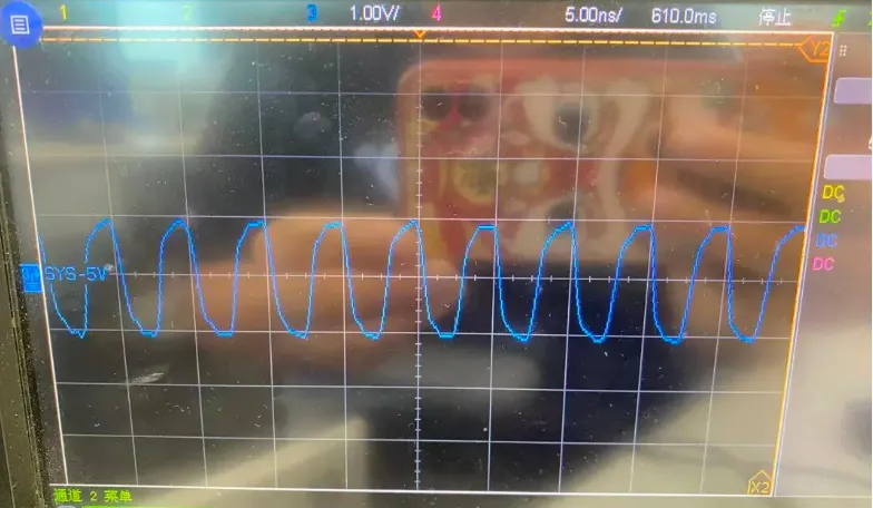
Power up the assembled PCB with a regulated 5V supply and use an oscilloscope to verify the signal generator output: expect a clean square wave with 40-50% duty cycle and minimal distortion. Measure amplifier gain by inputting a known signal and checking output amplitude, adjusting pots if included. Probe for ground bounce by comparing signal at source and load; excessive noise indicates poor decoupling. Test at maximum frequency to assess rise times; if ringing appears, add series resistors for damping. Common troubleshooting includes checking solder joints under magnification, verifying component values with a multimeter, and resimulating in PCB design software for layout errors. Systematic circuit testing confirms your electronics project meets high-speed goals.
If signals attenuate, review trace lengths and add shielding. Overheating in the amplifier suggests inadequate heatsinking or bias issues; measure quiescent current. For intermittent operation, inspect for mechanical stress on leads. These steps resolve most issues in a high-speed circuit PCB project.
Conclusion
This high-speed circuit PCB project demonstrates how hobbyists can create a functional signal generator and amplifier circuit using accessible tools and best practices. From schematic capture in PCB design software to soldering and rigorous circuit testing, each phase builds expertise in DIY PCB fabrication. Key takeaways include prioritizing signal integrity through controlled layouts and adherence to standards like IPC-2221C. Whether for testing other electronics projects or pure experimentation, this build delivers satisfaction and scalable knowledge. Experiment further by tweaking frequencies or adding filters to expand its utility.
FAQs
Q1: What makes a good PCB design software for a high-speed circuit PCB project?
A1: For electronic hobbyists, select PCB design software with strong routing tools, impedance calculators, and simulation integration. It should support multi-layer boards, auto-routing with constraints, and Gerber export. Free versions suffice for simple signal generator layouts, allowing quick iterations on trace widths and ground planes. Focus on user-friendly interfaces to avoid steep learning curves while ensuring compatibility with fab services.
Q2: How do I ensure reliable soldering in my DIY PCB amplifier circuit?
A2: Follow IPC J-STD-001J guidelines for joint formation, using quality solder and flux. Preheat boards, maintain iron tip temperature, and inspect for shiny fillets without bridges. Practice on scrap PCBs to master drag soldering for ICs. Clean thoroughly post-assembly to prevent ionic contamination affecting high-speed signals.
Q3: What are common pitfalls in circuit testing for electronics projects like this?
A3: Overlook ground loops or probe capacitance, which distort high-speed waveforms on oscilloscopes. Always use short ground springs and verify power supply ripple first. Simulate before building to catch schematic errors, and test incrementally: power, DC biases, then signals. This methodical approach saves time in troubleshooting signal generator issues.
Q4: Can beginners handle a high-speed circuit PCB project without advanced equipment?
A4: Yes, with basic tools like a multimeter, oscilloscope, and soldering station. Start at lower frequencies to validate, then push limits. Emphasize layout discipline over exotic materials. This DIY PCB project builds confidence for amplifier circuits and beyond.
References
IPC-2221C — Generic Standard on Printed Board Design. IPC, 2023
IPC J-STD-001J — Requirements for Soldered Electrical and Electronic Assemblies. IPC, 2024
IPC-A-600M — Acceptability of Printed Boards. IPC, 2025


