 ALLPCB


Beyond the Calculator: Advanced Considerations for Trace Width Design
In PCB design, engineers frequently rely on basic trace width calculators to meet current carrying needs. These tools provide a useful starting point, yet they often omit several critical variables that influence long term performance and reliability. Factors such as voltage drop along the conductor, reduced convective cooling at altitude, the complete absence of convection in vacuum, and the mechanical stresses unique to flexible substrates require additional analysis. Addressing these elements early in the layout process helps prevent overheating, signal integrity issues, and premature failure. The following discussion examines these considerations in detail for electrical engineers working on demanding applications.
Why Advanced Trace Width Considerations Matter
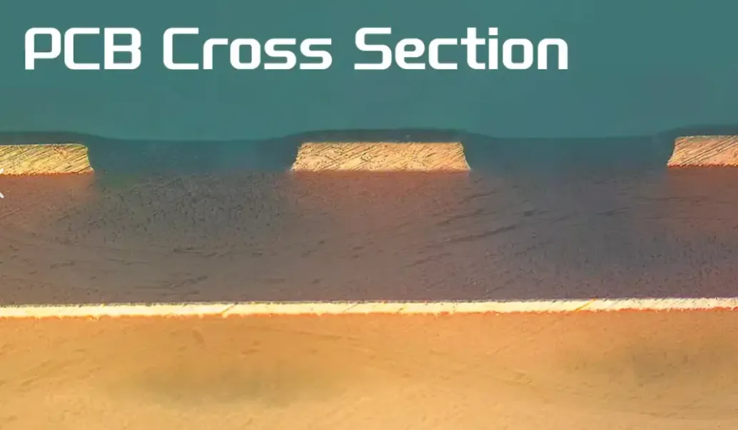
Trace width directly affects resistance, heat generation, and mechanical durability. When current flows through a copper conductor, the resulting voltage drop becomes significant in power distribution networks or precision analog circuits. At higher altitudes, lower air density impairs heat dissipation, forcing designers to increase trace width or add thermal relief features. In vacuum environments, heat removal occurs solely through conduction and radiation, altering the thermal balance entirely. Flexible circuits introduce cyclic bending that can crack narrow traces or delaminate copper from the substrate. Each of these conditions demands adjustments beyond standard room temperature, sea level calculations.
Technical Principles and Mechanisms
Voltage drop arises from the interaction of current, conductor length, cross sectional area, and copper resistivity, which itself varies with temperature. As current increases, resistive heating raises the trace temperature, further elevating resistance and creating a feedback loop that basic calculators may underestimate. Engineers therefore evaluate both steady state and transient conditions when specifying trace dimensions for pcb trace width voltage drop scenarios.
Altitude affects thermal performance because convective heat transfer depends on air density. Above approximately 3000 meters, the reduced mass of air molecules limits cooling efficiency, causing traces to run hotter for the same current. This phenomenon requires derating factors or wider traces to maintain acceptable temperature rise. In extreme cases, corona discharge can also appear at high voltages, influencing minimum spacing alongside width decisions.
In vacuum environments, the lack of any gaseous medium eliminates convection completely. Heat must escape through conduction into adjacent materials or radiation from the surface. Designers therefore consider emissivity of surface finishes and the thermal conductivity path to heat sinks or the board substrate. Trace width calculations shift emphasis toward minimizing self heating while ensuring adequate conduction paths, especially for high power traces.
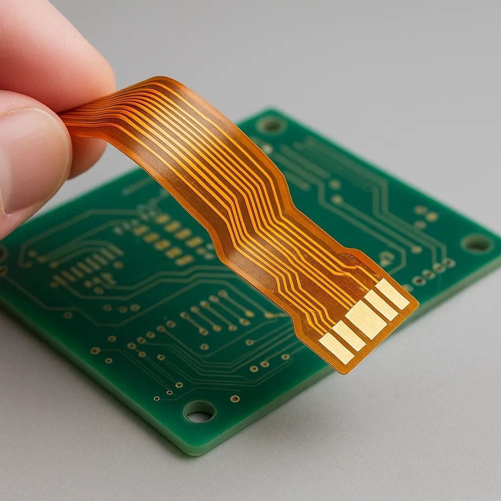
Flexible pcb trace width selection must account for strain during bending. When a circuit folds, the outer copper experiences tensile stress while the inner surface undergoes compression. Repeated flexing can initiate micro cracks that propagate over time, increasing resistance and eventually causing open circuits. Material properties such as copper ductility and adhesive strength between layers become relevant parameters alongside electrical requirements.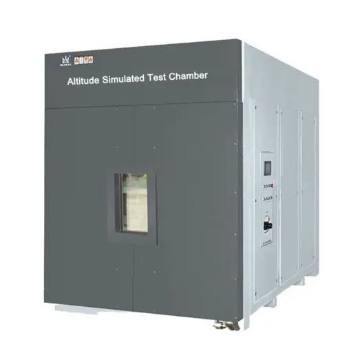
Practical Solutions and Best Practices
Begin with the base width from current carrying guidelines, then apply incremental adjustments for each environmental factor. For voltage drop, calculate the total resistance using the intended length and operating temperature, then verify that the resulting drop stays within system tolerances. When altitude derating applies, increase width proportionally or incorporate additional copper planes for heat spreading. In vacuum, prioritize low resistance paths and consider surface treatments that enhance radiative cooling.
For flexible circuits, maintain a minimum bend radius based on the number of layers and copper thickness. Place traces perpendicular to the bend axis where possible and avoid 90 degree turns in high flex zones. Staggered trace patterns or the addition of stiffeners in transition areas can further reduce localized strain. Verification through finite element thermal modeling combined with mechanical simulation provides higher confidence than calculator outputs alone.
Troubleshooting Insights for Complex Designs
When measured temperatures exceed predictions, re examine the assumptions used in the initial width calculation. Confirm actual copper thickness after plating, measure ambient conditions during testing, and verify that no unexpected current paths exist. In altitude or vacuum testing, incremental power ramp up helps isolate the point at which thermal limits are reached. For flexible assemblies, inspect failed units under magnification to determine whether cracks originated from bending stress or from manufacturing defects.
Conclusion
Basic trace width calculators serve as an efficient first approximation, yet they leave important variables unaddressed. Voltage drop, altitude effects, vacuum thermal behavior, and flexure induced stress each require targeted analysis. By incorporating these considerations systematically and validating against measured performance, engineers achieve designs that maintain electrical integrity and mechanical reliability across operating environments. Early attention to these factors reduces the need for costly revisions later in the development cycle.
FAQs
Q1: How does pcb trace width voltage drop influence power distribution networks?
A1: Voltage drop along a trace increases with current, length, and temperature while decreasing with greater cross sectional area. In power distribution, excessive drop can cause downstream components to receive insufficient voltage, leading to malfunction or reduced efficiency. Engineers calculate the expected drop at maximum load and operating temperature, then adjust width accordingly to keep the loss within acceptable limits for the application.
Q2: What trace width altitude considerations affect high altitude electronics?
A2: Lower air density at altitude reduces convective cooling, causing traces to operate at higher temperatures for a given current. Designers apply derating factors or increase width to maintain the same temperature rise as at sea level. Thermal modeling that incorporates reduced air pressure helps confirm that the final layout meets reliability targets.
Q3: How should trace width be approached in vacuum environments trace width applications?
A3: Without convection, heat removal relies on conduction and radiation. Traces must be sized to limit self heating while providing adequate conduction paths to heat sinks or thicker copper areas. Surface emissivity and board stack up play larger roles than in atmospheric designs, often requiring wider traces or additional thermal vias.
Q4: What factors determine flexible pcb trace width in dynamic applications?
A4: Bending introduces mechanical strain that can crack narrow traces over repeated cycles. Width selection balances electrical requirements against copper ductility and bend radius. Placing traces perpendicular to the bend line and avoiding sharp corners in flex zones helps maintain integrity throughout the product lifetime.


