 ALLPCB


Introduction
Traditional printed circuit boards dominate electronics manufacturing due to their reliability and scalability in producing flat, layered interconnects. Yet, the push for more integrated, lightweight, and custom-shaped devices challenges these conventional methods. Embedding components in 3D-printed electronics emerges as a transformative solution, where additive manufacturing processes directly incorporate passives, actives, and conductors into structural parts. This functional 3D printing enables seamless embedded electronics, reducing assembly steps and enabling complex geometries unattainable with standard PCBs. Electric engineers benefit from this shift by designing systems that merge mechanical strength with electrical performance in one build. As 3D printing PCBs evolves, it promises shorter lead times and greater design freedom for high-performance applications.
What Is Embedding Components in 3D-Printed Electronics and Why It Matters
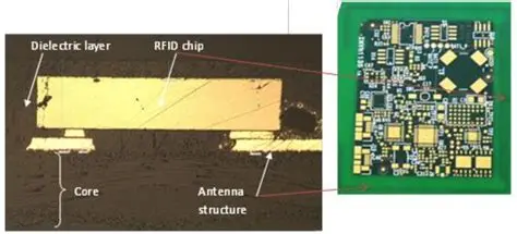
Embedding components in 3D-printed electronics involves integrating discrete elements like resistors, capacitors, sensors, and even microcontrollers directly into additively manufactured substrates during the printing process. Unlike surface-mount technology on PCBs, this method encapsulates components within polymer, ceramic, or composite matrices, creating monolithic devices. Techniques pause extrusion-based printing to insert off-the-shelf parts or print functional inks for custom passives. The result is additive manufacturing electronics that eliminate separate wiring and housing, ideal for conformal electronics on curved surfaces. This matters for electric engineers facing miniaturization pressures in IoT devices, wearables, and drones, where weight and volume constraints demand integrated solutions. Factory production gains efficiency, as multi-material printers handle both structure and circuitry in a single workflow.
The relevance intensifies in industries requiring harsh-environment resilience, such as aerospace, where embedded electronics withstand vibration without delamination. Traditional 3D printing PCBs often limits to prototypes, but advancing materials push toward production volumes. Engineers achieve higher component density, potentially reducing device footprints by integrating passives into substrates. Reliability improves through encapsulation, protecting against moisture and impact. Overall, this technology aligns manufacturing with design intent, minimizing supply chain complexities for custom embedded components 3D-printed electronics.
Technical Principles of Embedding Components
Core to this technology are extrusion-based methods like fused filament fabrication, where thermoplastic filaments form structural layers around placed components. During printing, the process pauses at precise heights, allowing manual or robotic insertion of surface-mount devices into cavities designed via slicing software. Resumption overprints insulation, securing parts mechanically and electrically. For printed-in-place elements, direct ink writing deposits conductive pastes for traces, resistive formulations for resistors, and dielectric inks for capacitors. Aerosol jet printing offers finer resolution, down to tens of microns, suitable for high-frequency signals in embedded electronics. These principles rely on material compatibility, with substrates like polyamide or ABS providing thermal stability during embedding.
Mechanical interlocking occurs as successive layers fuse around components, distributing stress across the volume rather than at joints. Electrical connectivity forms through printed vias or conductive adhesives bridging to traces. Challenges arise from coefficient of thermal expansion mismatches, where printed polymers expand differently from silicon dies, risking cracks under temperature cycles. Conductivity in printed traces, typically from silver or carbon fillers, lags behind copper foils but suffices for low-power applications. Factory insights emphasize layer adhesion, governed by print temperature and bed adhesion, to prevent voids that compromise functionality. Adherence to ASTM International standards for additive manufacturing ensures consistent process parameters across builds.
Passive component printing advances with multi-material systems, layering conductive, resistive, and insulating inks in registered stacks. Capacitors form by sandwiching high-k dielectrics between electrodes, while inductors coil helical traces. Active embedding requires heat-resistant parts to survive nozzle proximity, often using low-temperature solders or anisotropically conductive films for connections. Resolution limits print head size and ink viscosity, typically achieving 100-micron features for viable circuits. Vibration during printing demands stabilized platforms for precision placement. These mechanisms enable functional 3D printing, where the part itself conducts signals without added boards.
Challenges in Additive Manufacturing Electronics
Thermal management poses a primary hurdle, as embedded components generate heat trapped within insulating matrices, potentially exceeding polymer glass transition temperatures. Dissipation relies on high-thermal-conductivity fillers like graphene in substrates, yet airflow design becomes critical for sustained operation. Mechanical reliability suffers from anisotropic properties in printed parts, with layer interfaces weaker under shear than bulk material. Cyclic loading tests reveal delamination risks at component edges, necessitating reinforcement via fiber composites. Electrical performance degrades from trace resistance variations due to filler percolation thresholds in conductive filaments. Factory-driven validation involves accelerated aging to predict field failures.
Material selection balances printability, dielectric strength, and biocompatibility for medical uses. Hygroscopic inks absorb moisture, altering resistivity post-print, requiring controlled environments. Scalability limits stem from build volumes and print speeds, currently suiting prototypes over high-volume runs. Interfacing printed traces with standard connectors demands hybrid approaches, blending additive with subtractive processes. Standards like IPC-6012E qualification specs guide performance benchmarking against traditional PCBs. Addressing these ensures embedded components 3D-printed electronics meet engineering rigor.
Practical Solutions and Best Practices
Engineers optimize designs by simulating stress via finite element analysis, predicting warpage around embedded parts. Cavities feature draft angles for easy insertion, with tolerances at 0.1 mm for alignment. Multi-axis printing enhances conformal tracing on non-planar surfaces, improving signal integrity. Post-processing includes sintering inks for better conductivity and conformal coating for environmental sealing. Hybrid workflows combine printed passives with inserted actives, leveraging each process strengths. Factory protocols enforce cleanroom printing to avoid contamination on exposed pads.
Material qualification precedes production, testing filament shear strength and dielectric constants. Print parameters tune layer height to 0.1 mm for detail, with nozzle temperatures 220-250°C for engineering thermoplastics. Robotic pick-and-place integrates seamlessly during pauses, boosting throughput. Electrical testing post-embedding verifies continuity and insulation resistance per J-STD standards. Iterative prototyping refines workflows, ensuring yield above 90%. These practices enable reliable 3D printing PCBs in manufacturing pipelines.
For quality control, non-destructive inspection like X-ray reveals internal voids, while four-point probe measures trace resistance. Vibration tables simulate operational stresses, aligning with ISO 9001 quality systems. Documentation tracks material batches for traceability. Scaling involves parallel printer farms, with software automating G-code for component placement. Collaboration between design and manufacturing teams accelerates adoption of additive manufacturing electronics.
Real-World Insights from Manufacturing
In structural health monitoring, sensors embedded in drone wings detect strain without added mass, printed via direct ink writing for wireless transmission. Automotive prototypes integrate capacitors into conformal housings, reducing wiring harnesses by half. Medical wearables embed ECG electrodes in flexible substrates, conforming to body contours. These examples highlight factory transitions, where initial prototypes evolve to low-volume series via validated processes. Engineers troubleshoot via cross-sections, adjusting infill density for thermal paths. Success hinges on multidisciplinary expertise, blending electronics with AM principles.
Conclusion
Embedding components in 3D-printed electronics transcends traditional PCBs, fostering integrated, multifunctional devices through additive manufacturing. Key benefits include design freedom, reduced assembly, and enhanced durability for demanding applications. Technical challenges like thermal mismatch and material limits yield to optimized processes and standards compliance. Electric engineers gain tools for innovation, from custom passives to fully encapsulated systems. As functional 3D printing matures, factories position for efficient production of embedded electronics. This evolution redefines electronics manufacturing, prioritizing integration over layering.
FAQs
Q1: What are the main techniques for embedded components 3D-printed electronics?
A1: Primary methods include pausing fused filament fabrication to insert components, direct ink writing for printed traces and passives, and aerosol jet for high-resolution features. These enable seamless integration into structural parts. Factory practices emphasize precise cavity design and material matching to ensure mechanical lock-in and electrical connectivity. Alignment with ASTM additive manufacturing standards supports repeatable outcomes for engineering applications.
Q2: How does 3D printing PCBs differ from embedding electronics?
A2: 3D printing PCBs focuses on layered circuit boards via additive traces, while embedding incorporates components directly into volumetric structures. The latter achieves true functional 3D printing by merging mechanics and electronics. Challenges involve thermal management, addressed through conductive fillers. Benefits include miniaturization for wearables, with processes validated against IPC performance specifications.
Q3: What challenges arise in additive manufacturing electronics reliability?
A3: Key issues encompass expansion mismatches causing cracks, limited trace conductivity, and layer delamination under stress. Solutions feature simulation-driven designs and post-sintering. Factory testing includes thermal cycling per J-STD guidelines to verify longevity. This ensures embedded electronics withstand operational demands in real-world deployments.
Q4: Can functional 3D printing replace traditional PCBs entirely?
A4: Not yet for high-volume, high-speed apps, but excels in custom, low-volume integrated devices. Hybrid approaches combine both for optimal results. Standards guide qualification, enhancing trust. Engineers leverage it for prototypes evolving to production where conformal shapes matter.
References
IPC-6012E — Qualification and Performance Specification for Rigid Printed Boards. IPC, 2017
ISO/ASTM 52900 — Additive manufacturing — General principles — Fundamentals and vocabulary. ISO/ASTM, 2015
J-STD-020E — Moisture/Reflow Sensitivity Classification of Nonhermetic Surface Mount Devices. JEDEC, 2014
ASTM F42 — Additive Manufacturing Technologies Committee Standards. ASTM International


