 ALLPCB


Introduction
Line width tolerance and PCB layer stackup form the core elements that determine the reliability and efficiency of printed circuit boards in high-performance applications. Electrical engineers must prioritize these factors to ensure signal integrity, controlled impedance, and overall board functionality. Variations in trace width during manufacturing can directly impact electrical characteristics, while the layer stackup dictates how signals propagate through the board. PCB material properties, such as dielectric constant, play a critical role in maintaining consistent performance across layers. This article explores the interplay between line width tolerance and PCB layer stackup, offering structured insights for optimizing designs. Understanding these fundamentals helps engineers achieve robust signal layer configurations that meet demanding operational requirements.
What Is Line Width Tolerance and Why It Matters
Line width tolerance refers to the allowable deviation between the designed trace width and the actual width produced during PCB fabrication. This tolerance arises from etching processes, copper thickness variations, and material interactions, typically specified as a percentage of the nominal width. For instance, tighter tolerances are essential in high-frequency designs where even small deviations can alter electrical performance. In the context of IPC-A-600, acceptability criteria ensure that conductor widths meet minimum standards to prevent failures like shorts or opens. Engineers must consider line width tolerance early in the design phase because it influences current-carrying capacity and thermal management. Poor tolerance control can lead to inconsistent trace width impedance, compromising the entire board's reliability.
The relevance of line width tolerance extends to multilayer boards, where it interacts with the overall stackup. Wider tolerances increase the risk of impedance mismatches, especially in controlled-impedance traces used for high-speed signals. This directly affects signal layer configuration, as outer and inner layer traces respond differently to manufacturing variations. By adhering to established guidelines, engineers can predict and mitigate these effects, ensuring the board performs as intended under operational stresses. Ultimately, precise line width tolerance supports the foundation of performance by enabling predictable electrical behavior across the PCB.
Understanding PCB Layer Stackup
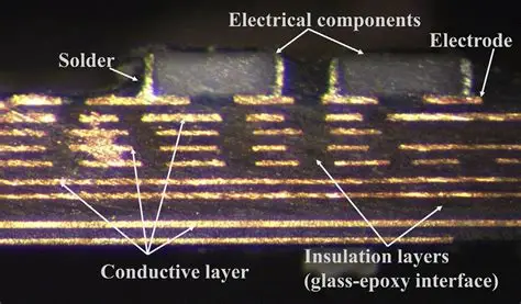
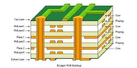
PCB layer stackup defines the sequential arrangement of conductive layers, dielectric materials, and planes in a multilayer board. It includes signal layers, power planes, ground planes, and prepregs, each contributing to mechanical stability and electrical isolation. The configuration determines signal propagation speed, crosstalk levels, and heat dissipation paths. Key PCB material properties, like dielectric constant and thickness, vary between core and prepreg layers, influencing the overall stackup symmetry. Engineers design stackups to balance manufacturing feasibility with performance needs, often prioritizing adjacent reference planes for signal layers. A well-planned PCB layer stackup minimizes warpage and ensures uniform thickness control throughout production.
In high-density designs, the stackup directly governs trace width impedance through the proximity of reference planes and dielectric heights. Asymmetric stackups can introduce unwanted resonances or increase insertion loss, particularly at gigahertz frequencies. Signal layer configuration within the stackup optimizes routing density while maintaining isolation between adjacent traces. Material selection for each layer must account for thermal expansion coefficients to prevent delamination during assembly. By methodically engineering the stackup, designers achieve the desired electrical characteristics without excessive iterations.
The Interplay Between Line Width Tolerance and Stackup
Line width tolerance becomes critical when integrated with PCB layer stackup, as trace dimensions directly influence characteristic impedance. Impedance formulas incorporate trace width, dielectric height to the nearest reference plane, dielectric constant, and copper thickness, making stackup parameters interdependent. A deviation in line width, say due to etching undercuts, shifts the impedance profile, potentially causing reflections in high-speed signals. Engineers must model these interactions using stackup-specific data to predict tolerance impacts. PCB material properties, particularly the dielectric constant of prepregs and cores, amplify these effects in inner layers where tolerances are harder to control.
In signal layer configurations, outer layers often tolerate wider line width variations compared to inner layers buried deeper in the stackup. The dielectric constant affects field distribution around the trace, so materials with stable Er values enhance tolerance margins. Stackup symmetry helps distribute manufacturing variations evenly, reducing bow and twist that could exacerbate width inconsistencies. Per IPC-6012 guidelines, performance specifications demand that conductor widths align with design intents to uphold electrical integrity. This interplay underscores why engineers simulate stackups with tolerance bands during the design verification process. Proactive management ensures the foundation of performance remains solid across production runs.
Technical Principles of Impedance Control in Stackups
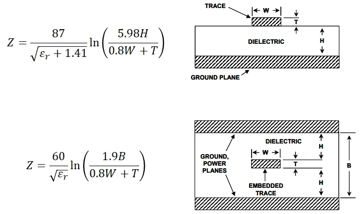
Characteristic impedance in PCB traces arises from the interaction of inductance and capacitance, shaped by the layer stackup geometry. Trace width determines the conductor's contribution to these parameters, while dielectric constant sets the capacitive coupling strength. The height between a signal trace and its reference plane, defined by the stackup, critically tunes impedance values. Variations in line width tolerance alter the effective width, shifting impedance by percentages proportional to the deviation. For microstrip configurations on outer layers, air's low dielectric constant supplements the substrate Er, demanding precise width control.
In stripline setups within the stackup, dual dielectric interfaces enclose the trace, making impedance more sensitive to material properties and thickness uniformity. Engineers calculate nominal impedance assuming ideal tolerances, then apply margins based on manufacturing capabilities. Signal layer configuration often pairs differential pairs with symmetric stackups to maintain common-mode rejection. PCB material properties like loss tangent further influence high-frequency performance, where tolerance-induced mismatches amplify attenuation. Adhering to IPC-2221 principles for multilayer design guides these calculations, ensuring robust impedance control. These technical mechanisms highlight the foundational role of stackup and tolerance in achieving predictable signal behavior.
Best Practices for Optimizing Line Width Tolerance and Stackup
Start stackup design by selecting materials with consistent dielectric constant and low variation in properties across suppliers. Specify line width tolerances explicitly in fabrication drawings, targeting 10-15% for standard designs and tighter for impedance-controlled traces. Use symmetric stackups for boards exceeding six layers to minimize warpage and maintain reference plane efficacy. Simulate impedance across tolerance ranges using stackup cross-sections to validate signal layer configurations. Collaborate with fabricators early to align on achievable tolerances based on copper weights and etching processes.
Incorporate ground planes adjacent to high-speed signal layers to stabilize impedance despite width variations. Opt for thinner dielectrics in critical stackup regions to reduce the impact of width tolerances on overall Z0. Verify PCB material properties through datasheets specifying Er at operating frequencies. Employ design rules that enforce minimum spacings scaled to tolerance expectations. Regular automated optical inspections post-etching confirm line width adherence before lamination. These practices build a performance foundation resilient to manufacturing realities.
Common Challenges and Troubleshooting Insights
Engineers often encounter impedance drift in prototypes due to unaccounted line width tolerances in asymmetric stackups. Signals exhibit ringing or eye closure when actual widths narrow beyond 85% of design, as seen in high-density interconnects. Troubleshooting involves sectioning boards to measure dielectric heights and Er via time-domain reflectometry. Misaligned signal layer configurations exacerbate crosstalk if tolerances vary layer-to-layer. Adjust by redesigning stackups with balanced prepreg counts and wider nominal traces.
Another issue arises from material hygroscopicity altering dielectric constant post-lamination, compounding width effects. Bake boards pre-assembly to stabilize properties, then retest impedance. Warpage in thick stackups distorts trace geometries, demanding core-prepreg matching per CTE guidelines. Case analyses reveal that symmetric 12-layer stackups with 12% width tolerance yield 5-8% impedance variation, acceptable for most RF applications. Systematic root-cause analysis ties back to stackup planning, reinforcing proactive design.
Conclusion
Line width tolerance and PCB layer stackup underpin PCB performance by governing impedance, signal integrity, and mechanical reliability. Engineers achieve optimal results through precise material selection, symmetric configurations, and tolerance-aware simulations. Integrating dielectric constant and PCB material properties ensures consistent trace width impedance across layers. Adopting best practices minimizes risks, fostering designs that excel in demanding environments. This foundation empowers electrical engineers to deliver high-performance boards reliably.
FAQs
Q1: What role does dielectric constant play in PCB layer stackup?
A1: Dielectric constant influences signal speed and impedance in the PCB layer stackup by determining capacitive coupling between traces and planes. Lower Er values enable faster propagation in high-speed designs, while stable properties across frequencies maintain consistency. Engineers select materials matching the stackup's dielectric heights to control trace width impedance effectively. Proper integration prevents mismatches that degrade performance.
Q2: How does trace width impedance relate to signal layer configuration?
A2: Trace width impedance depends on signal layer configuration within the stackup, including proximity to reference planes and dielectric thicknesses. Narrower widths increase impedance, suiting certain high-frequency needs, while wider ones lower it for power delivery. Tolerances must align with configuration to avoid reflections. Simulations verify compatibility before fabrication.
Q3: Why are PCB material properties critical for line width tolerance?
A3: PCB material properties like dielectric constant and CTE affect how line width tolerances impact overall board integrity. Variations in Er alter field distribution around traces, amplifying impedance shifts from width deviations. Matching properties across stackup layers ensures uniform performance. This controls thermal stresses that could warp traces further.
Q4: What best practices improve PCB layer stackup for performance?
A4: Prioritize symmetric PCB layer stackups with adjacent ground planes for signal layers to stabilize impedance despite line width tolerances. Select materials with low Dk variation and verify via stackup models. Specify tight tolerances for critical traces and inspect post-etch. This approach optimizes signal integrity reliably.
References
IPC-A-600K — Acceptability of Printed Boards. IPC, 2020
IPC-6012E — Qualification and Performance Specification for Rigid Printed Boards. IPC, 2017
IPC-2221B — Generic Standard on Printed Board Design. IPC, 2012
IPC-4101E — Specification for Base Materials for Rigid and Multilayer Printed Boards. IPC, 2010


