 ALLPCB


Introduction
Rigid-flex PCBs integrate rigid and flexible sections into a single board, enabling compact designs for applications like medical devices, aerospace systems, and consumer electronics. These boards offer superior reliability in dynamic environments compared to purely rigid or flexible alternatives. However, their fabrication involves complex materials and processes, driving up costs significantly over standard rigid boards. Engineers often face the challenge of rigid-flex PCB cost optimization without sacrificing electrical performance or mechanical integrity. This article provides factory-driven insights into affordable rigid-flex design strategies, focusing on flex PCB cost reduction techniques that align with industry standards. By applying these principles, design teams can minimize rigid-flex PCB expenses while meeting stringent performance requirements.
Understanding Rigid-Flex PCBs and Their Cost Implications
Rigid-flex PCBs consist of rigid substrates, typically made from epoxy-based laminates, bonded to flexible polyimide circuits through adhesives or direct lamination. The flexible regions allow bending and folding, reducing connector needs and assembly steps in space-constrained products. Factory production classifies them under standards like IPC-6013, which specifies qualification for flexible and rigid-flex boards to ensure consistent performance. Cost matters because flex materials and multi-step lamination increase expenses by factors related to layer count and panel yield. In high-volume manufacturing, poor design choices amplify waste, making rigid-flex PCB cost optimization essential for project viability. Engineers must weigh these factors early to balance budget constraints with reliability demands.
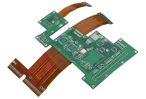
The relevance stems from growing demand in miniaturized electronics, where rigid-flex solutions replace wired harnesses but at a premium. Procurement teams scrutinize expenses tied to material waste, tooling, and testing. Without targeted flex PCB cost reduction, projects exceed budgets, delaying market entry. Factory insights reveal that up to 70% of costs trace to design decisions, underscoring the need for proactive optimization. Affordable rigid-flex design thus becomes a competitive edge for engineering teams.
Key Technical Principles Driving Costs in Rigid-Flex Design
Material selection forms the foundation of cost in rigid-flex PCBs, with polyimide films for flex areas costing more than FR4 for rigid sections due to their thermal stability and flexibility. Copper foil weight in flex regions must be optimized, as heavier foils increase material use and bending stress. Adhesive layers between rigid and flex require precise control to avoid delamination, adding process complexity. IPC-2223 outlines design rules for these interfaces, including bend radius minima to prevent cracking during flexure. Stackup configuration influences yield, as mismatched CTEs between materials cause warpage in multi-layer builds. These principles directly impact minimizing rigid-flex PCB expenses through efficient engineering.
Layer count amplifies costs exponentially, since each additional layer demands extra lamination cycles and registration accuracy. Vias transitioning from rigid to flex zones require blind or buried types to maintain signal integrity, but they elevate drilling and plating expenses. Panel utilization suffers from irregular outlines, leading to scrap in high-volume runs. Factory processes emphasize symmetrical stackups to reduce asymmetry-induced defects. Understanding these mechanisms allows engineers to target interventions for rigid-flex PCB cost optimization.
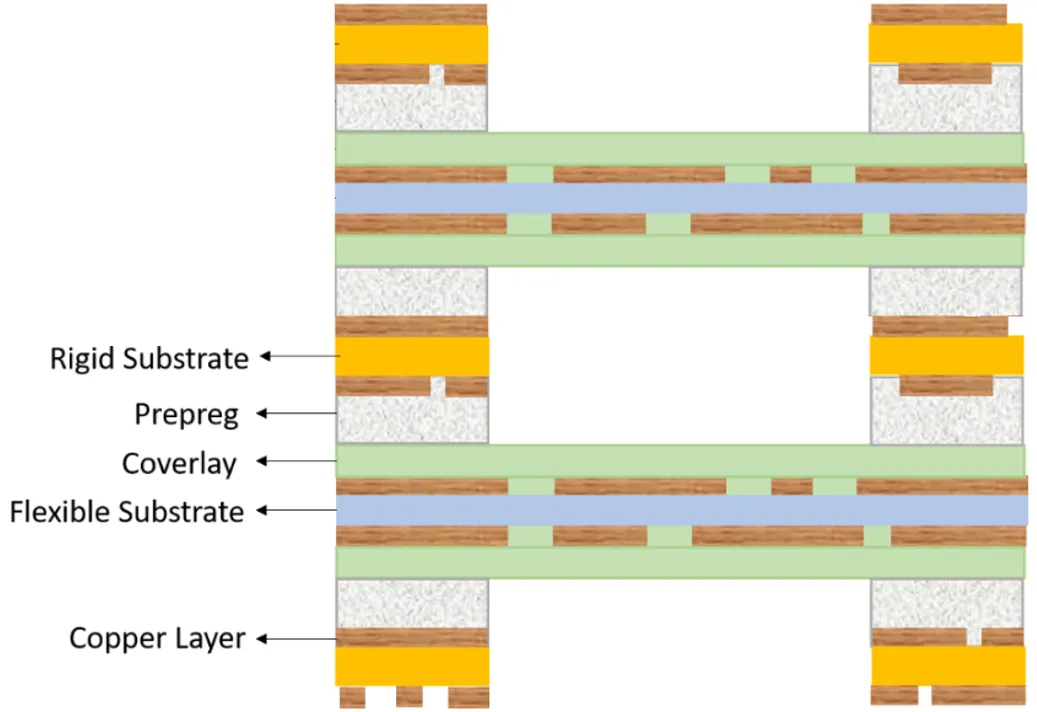
Bend radius and strain distribution in flex arms dictate reliability, with tighter radii risking copper fatigue over cycles. Standards like IPC-2223 specify minimum radii based on copper thickness, guiding cost-effective routing. Thermal management adds cost via high-Tg materials if reflow demands exceed basics. These interconnected principles require holistic design review to achieve flex PCB cost reduction without performance trade-offs.
Best Practices for Affordable Rigid-Flex Design
Start with minimizing flex area size, as flex materials dominate expenses; limit flex sections to essential interconnects between rigid islands. This reduces polyimide usage and simplifies lamination. Optimize layer count by consolidating signals on fewer layers through dense routing and embedded passives where feasible. Factory experience shows that designs under six total layers often cut costs by streamlining presses. Incorporate design for manufacturability early, such as standard panel sizes for nesting multiple boards. These steps form the core of affordable rigid-flex design.
Material choices should prioritize standard polyimides and FR4 grades available in volume, avoiding exotic high-frequency dielectrics unless critical. Select copper weights like 1 oz for flex to balance conductivity and bend endurance. Use coverlay instead of soldermask on flex for better flexibility at lower cost in some cases. Stiffeners should be FR4 frames only where needed, preferring polyimide for lighter applications. IPC-6013 compliance ensures these selections yield reliable boards without excess testing. Such factory-aligned picks drive flex PCB cost reduction.
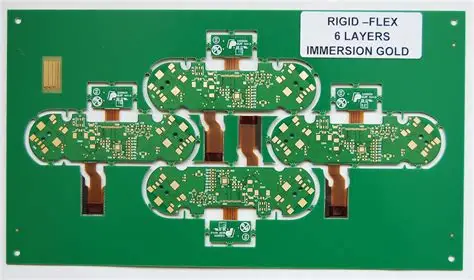
Routing optimization reduces vias and trace lengths, minimizing plating steps. Group signals by bend zones to shorten flex arms, cutting material. Employ teardrop pads and larger annular rings per IPC-2223 to boost yield and avoid drill breakage. Surface finishes like ENIG should be reserved for high-reliability needs; HASL or OSP suffice for cost-sensitive builds. Test points and fiducials aid assembly without added layers. These practices enable minimizing rigid-flex PCB expenses systematically.
In fabrication, specify sequential lamination to build rigid sections around flex cores, reducing alignment errors. Avoid bookbinder construction unless bend complexity demands it, as it hikes tooling. Panelize designs with scored edges for depaneling efficiency. Post-process controls like baking prevent moisture issues per JEDEC guidelines. Volume quoting reveals further savings through annual contracts. Comprehensive DFM reviews integrate these for peak rigid-flex PCB cost optimization.
Real-World Application: Optimizing a Wearable Device PCB
Consider a wearable health monitor requiring rigid-flex for battery and sensor integration. Initial design used eight layers with full-flex tails, inflating costs via excess polyimide. Optimization reduced flex to interconnect strips, dropped to five layers, and nested four boards per panel. Material swaps to standard polyimide cut 25% off raw costs, while IPC-2223-guided routing halved vias. Factory trials confirmed IPC-6013 qualification with no delams after 10,000 bends. Final prototype achieved flex PCB cost reduction, fitting budget while retaining signal integrity.
This case highlights iterative DFM, where simulation tools predict warpage before fab. Strain analysis ensured coverlay integrity. Procurement aligned with volume tiers for further discounts. Such insights scale to aerospace or automotive uses. Engineers replicate this by prioritizing flex minimization and standard processes.
Conclusion
Cost-effective flex-to-rigid PCB design hinges on strategic material use, simplified stackups, and DFM integration. By limiting flex extent, optimizing layers, and adhering to IPC standards, teams realize substantial savings. Factory-driven practices like efficient nesting and standard finishes compound benefits in production. Balancing performance through bend-compliant routing maintains reliability. Implementing these for rigid-flex PCB cost optimization empowers projects to thrive within budgets. Future designs will leverage these timeless principles amid evolving tech demands.
FAQs
Q1: How can engineers achieve rigid-flex PCB cost optimization in early design stages?
A1: Focus on minimizing flex area and layer count while using standard materials like polyimide and FR4. Apply IPC-2223 rules for routing and bends to avoid yield losses. Nest panels efficiently and review DFM with fabricators. These steps reduce material waste and process steps, typically lowering costs without performance hits. Factory validation confirms viability before full runs.
Q2: What are proven flex PCB cost reduction techniques for high-volume manufacturing?
A2: Prioritize sequential lamination, standard copper weights, and coverlay over soldermask in flex zones. Optimize vias with blind types and teardrops per standards. Choose cost-effective finishes like OSP. Panel utilization via simple outlines cuts scrap. Align with IPC-6013 for qualification, ensuring scalability. These yield 20-30% savings in mature processes.
Q3: Why is affordable rigid-flex design challenging, and how to overcome it?
A3: Challenges arise from material premiums and lamination complexity, amplifying per-board costs. Overcome by consolidating layers, shortening flex arms, and standardizing stackups. Simulate CTE mismatches to prevent warpage. Engage factories early for quoting insights. This minimizes rigid-flex PCB expenses while meeting reliability per IPC guidelines.
Q4: What role do standards play in minimizing rigid-flex PCB expenses?
A4: Standards like IPC-2223 and IPC-6013 guide efficient designs, reducing iterations and defects. They specify bend radii and qualifications, avoiding over-engineering. Compliance streamlines quoting and testing, cutting hidden costs. Factory adherence boosts yield, directly aiding flex PCB cost reduction.
References
IPC-2223E — Sectional Design Standard for Flexible/Rigid-Flexible Printed Boards. IPC
IPC-6013 — Qualification and Performance Specification for Flexible Printed Boards. IPC
JEDEC J-STD-020E — Moisture/Reflow Sensitivity Classification. JEDEC





