 ALLPCB


Introduction
Compact PCB design represents a critical challenge in modern electronics, where devices demand ever-smaller footprints without sacrificing performance or reliability. Electrical engineers face the task of packing more components into limited spaces while ensuring the board remains manufacturable at scale. High-density interconnect (HDI) PCB design emerges as a key solution, enabling finer features like microvias and thinner traces. However, pushing component density too far can lead to fabrication issues, yield losses, and assembly failures. This article explores strategies to balance these competing priorities, drawing on established engineering principles. By integrating component placement strategies for small PCBs, optimized routing, and design for manufacturability (DFM) guidelines, designers can achieve robust, high-performance boards.
Why Compact PCB Design Matters in Today's Electronics
The drive toward miniaturization stems from consumer demands for portable, efficient devices across sectors like telecommunications, medical equipment, and automotive systems. Traditional PCBs struggle to meet these needs due to limitations in routing density and interlayer connections. HDI PCB design addresses this by incorporating advanced features that support ball grid arrays (BGAs) with pitches below 0.5 mm and multilayer stackups exceeding 10 layers. Yet, manufacturability remains a bottleneck; overly aggressive designs often result in defects like via failures or trace shorts during production. Engineers must weigh the benefits of increased functionality against real-world fabrication constraints. Adhering to DFM guidelines early prevents costly redesigns and ensures consistent quality.
In high-volume production, even minor density improvements translate to significant space savings, but only if the design aligns with standard processes. For instance, compact layouts reduce overall system size, enabling sleeker enclosures and better thermal management. The interplay between density and manufacturability defines project success, as poor choices amplify risks in signal integrity and mechanical stress.
Core Principles of High-Density Interconnect (HDI) PCB Design
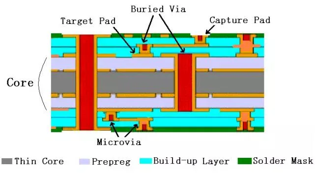
HDI PCB design relies on microvias, typically laser-drilled with diameters under 150 microns, to create shorter interconnect paths and higher layer counts. These structures, classified into types like 1+n+1 or 2+n+2 per IPC-2226A, allow blind and buried vias that do not span the full board thickness. This approach minimizes signal propagation delays and electromagnetic interference in dense environments. Engineers select HDI when component counts exceed conventional limits, such as in processors with thousands of I/Os. However, material selection and stackup planning become paramount to control impedance and thermal expansion. Sequential lamination processes build these boards layer by layer, demanding precise registration to avoid misalignment.
Layer stackups in HDI designs often feature thin dielectrics, around 50 microns, to support tight via aspect ratios. Core materials must exhibit low coefficient of thermal expansion to prevent warpage under reflow. Power and ground planes integrate seamlessly, providing return paths and shielding. Designers simulate these configurations to verify electrical performance before fabrication. The result is a board capable of handling gigahertz signals in a fraction of the space of standard multilayers.
Component Placement Strategies for Small PCBs
Effective component placement strategies for small PCBs prioritize signal flow, thermal dissipation, and assembly efficiency. Begin by positioning high-speed components near connectors to shorten critical traces and reduce stubs. Group analog and digital sections to minimize noise coupling, maintaining at least 1 mm separation where possible. Fixed elements like connectors anchor the layout, with subsequent parts oriented for unidirectional assembly flows. This reduces pick-and-place errors and optimizes solder paste application. Symmetry in placement across the board mitigates warpage risks during lamination and reflow.
In compact designs, utilize the board edges for taller components, reserving the center for flat ICs and passives. Employ fiducials and panelization thoughtfully to aid alignment without wasting real estate. Simulate airflow early to identify hot spots, adjusting placements to enhance natural convection. For BGAs, ensure via-in-pad compatibility to escape signals efficiently. These strategies not only boost density but also streamline downstream processes. Balancing proximity for performance with spacing for accessibility proves essential.
Consider decoupling capacitors placed within 1-2 mm of power pins to stabilize supplies in dense arrays. Rotate components to align pads parallel, easing routing. Avoid clustering heat-generating parts, distributing them evenly. Such deliberate planning transforms constrained spaces into functional powerhouses.
Optimizing Trace Width and Spacing in High-Density Layouts
Optimizing trace width and spacing forms the backbone of reliable high-density routing. Trace widths scale with current demands, typically 75-100 microns for signals and wider for power delivery, per IPC-2152 guidelines for thermal management. Spacing prevents arcing and crosstalk, with minimums of 50-75 microns in inner layers to accommodate etching tolerances. Engineers calculate these using stackup-specific cross-section analysis, factoring in copper weight and dielectric constants. Tighter geometries demand finer photoresist and plasma cleaning for clean definition. Consistent line-to-space ratios, like 1:1, enhance yield.
Impedance control guides outer layer traces, often using differential pairs with controlled gaps. Avoid 90-degree bends, opting for 45-degree miters to reduce reflections. Fill unused areas with ground pours, stitching them to planes via vias. High-speed nets receive priority routing on dedicated layers. These practices maintain signal integrity amid density pressures. Verification through DRC and length matching ensures compliance.
In HDI, microstrip and stripline configurations dominate, with spacing adjusted for fringing fields. Simulate eye diagrams to validate margins. Progressive narrowing near pins maximizes fanout density. Such optimization yields robust interconnects.

Via Selection for Compact Layouts
Via selection for compact layouts hinges on size, type, and placement to minimize inductance while preserving density. Microvias suit HDI, offering 0.1 mm diameters and aspect ratios under 1:1 for reliable plating. Blind vias connect adjacent layers without penetrating the core, ideal for BGA escapes. Stacked vias build vertical interconnects in buildup layers, but require sequential processing to fill reliably. Buried vias free surface space, hidden within the stackup. Selection aligns with layer count and pitch requirements.
Aspect ratio limits plating uniformity, typically capped at 0.8:1 in production. Via-in-pad designs embed vias directly under components, demanding filled or tented finishes. Annular ring sizes, around 75 microns, prevent breakout during drill. Distribution patterns avoid clustering to control stress concentrations. IPC-2226A outlines these parameters for HDI viability. Proper tenting and back-drilling enhance performance.
Trade-offs include cost versus density; staggered vias reduce layers but complicate routing. Simulate thermal cycling to predict reliability. These choices enable seamless integration in tight spaces.
Design for Manufacturability (DFM) Guidelines for Compact PCBs
DFM guidelines bridge design intent and production reality, emphasizing rules like minimum annular rings and drill sizes. Panel utilization maximizes throughput, with v-scoring or tab routing for depanelization. Solder mask expansion over pads prevents bridging, typically 50-75 microns. Legend placement avoids trace overlaps, using durable inks. Fiducial accuracy, within 25 microns, supports vision systems. Copper balance across layers prevents bow and twist.
Fabricators prefer standard thicknesses, like 0.8 mm cores, to leverage existing tooling. Aspect ratios under 10:1 for through-holes ease plating. Test point access remains mandatory for in-circuit verification. These guidelines, rooted in IPC-2221, reduce iterations. Early DFM reviews catch issues like insufficient clearance.
Bake-out provisions handle moisture sensitivity, aligning with assembly profiles. Such proactive measures ensure first-pass success.
Common Challenges and Troubleshooting in Compact Designs
Engineers often encounter warpage in HDI boards due to asymmetric stackups, addressed by core compensation and symmetric builds. Signal crosstalk in fine-pitch routing requires shielding and guard traces. Via reliability under thermal stress demands aspect ratio checks and plating thickness verification. Component shadowing during reflow calls for stencil optimizations. Troubleshooting involves CAE simulations and prototype cross-sections. Iterative feedback refines designs.
Case in point: A 12-layer HDI for a handheld device suffered yield drops from microvia cracks. Adjusting dielectric thickness and via stagger resolved it, boosting density without rework.
Conclusion
Mastering compact PCB design demands a holistic approach, integrating HDI innovations with disciplined placement, routing, and DFM adherence. Electrical engineers who optimize trace width and spacing, select vias judiciously, and follow component strategies achieve superior density and reliability. Standards like IPC-2226A and IPC-2221 provide the framework for success. Ultimately, this balance unlocks smaller, smarter electronics without compromising manufacturability. Prioritize simulation and collaboration for optimal outcomes.
FAQs
Q1: What are the key benefits of high-density interconnect (HDI) PCB design for compact devices?
A1: HDI enables finer pitches and shorter paths, supporting advanced components in minimal space. Microvias reduce inductance, improving signal speed. Layer buildup accommodates complex routing without increasing board size. This suits wearables and IoT, balancing performance and footprint logically.
Q2: How do component placement strategies for small PCBs impact manufacturability?
A2: Strategic grouping shortens traces and aids assembly flow, reducing errors. Edge placement for connectors eases handling. Thermal distribution prevents hotspots. These align with DFM, ensuring high yields in production.
Q3: What factors influence via selection for compact layouts?
A3: Size, type, and aspect ratio determine density and reliability. Microvias fit HDI, while stacked configurations build height. Annular rings and fill methods affect plating. Select based on stackup for optimal performance.
Q4: Why is optimizing trace width and spacing critical in HDI designs?
A4: It prevents shorts, controls impedance, and manages heat. Minimums accommodate fab tolerances. Calculations per standards ensure current capacity. This maintains integrity in dense routing.


