 ALLPCB


Introduction
While FR-4 substrates dominate rigid PCB manufacturing due to their stability and cost-effectiveness, flexible and rigid-flex PCBs open new possibilities for compact, dynamic applications in wearables, medical devices, and aerospace systems. These boards use materials like polyimide films that allow bending and folding, but panelization, the process of arraying multiple circuits on a single production panel, introduces unique challenges. Unlike rigid panels, flexible materials are prone to warping, tearing, and handling damage during fabrication, assembly, and depaneling. Electrical engineers must address these issues to optimize yield, reduce costs, and ensure reliability in high-volume production. This article explores key considerations for flexible PCB panelization and rigid-flex PCB panel design, focusing on practical strategies aligned with industry practices.
What Is Flexible and Rigid-Flex PCB Panelization and Why It Matters
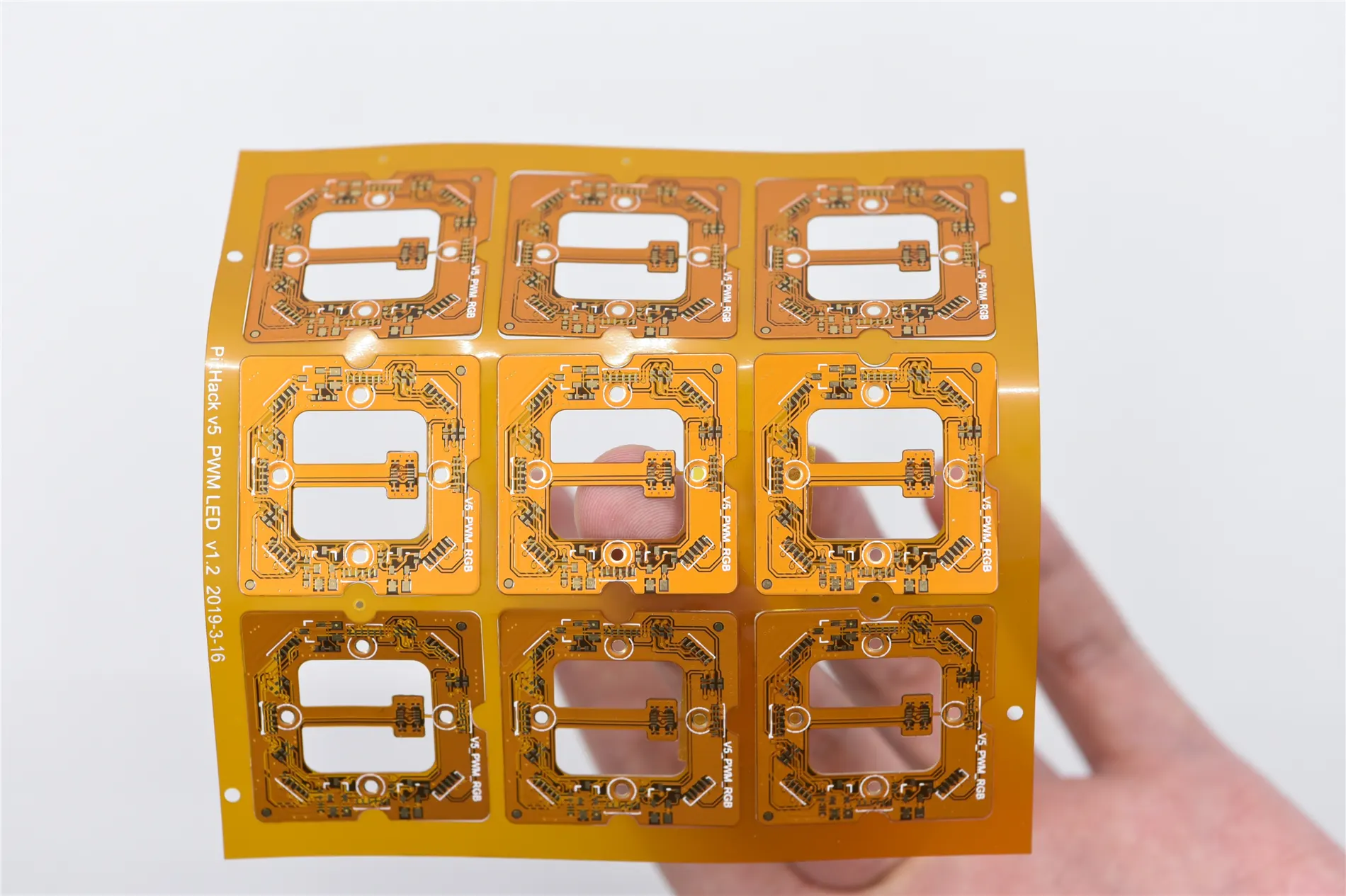
Panelization involves grouping multiple individual PCB designs onto a larger panel to streamline manufacturing processes such as etching, plating, and soldering. For flexible PCBs, this means arranging thin, bendable circuits on a carrier or frame to maintain planarity during handling. Rigid-flex panels combine rigid sections, typically FR-4 based, with flexible interconnects, requiring hybrid layouts that protect both material types. The primary goal is to maximize material utilization while minimizing waste and processing time. In high-volume runs, effective panelization can cut per-unit costs by 20 to 50 percent through better throughput, but poor design leads to scrap from flex damage or misalignment.
These considerations matter because flexible materials lack the mechanical rigidity of FR-4, making them susceptible to stress during automated handling. Engineers face trade-offs between panel density and structural integrity, especially in surface-mount technology assembly where fiducials and tooling holes must align precisely. For rigid-flex, panelization ensures the transition zones between rigid and flex areas remain intact, preserving signal integrity and mechanical durability. Ultimately, thoughtful panelization supports scalable production while meeting performance demands in space-constrained environments.
Challenges in Handling Flexible Materials During Panelization
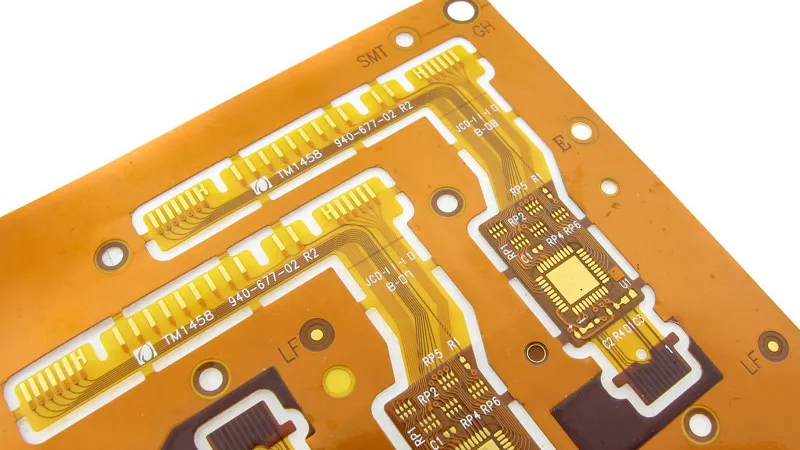
Flexible PCBs typically feature substrates as thin as 25 to 125 micrometers, with copper foils and coverlays that enable repeated bending but complicate panel processing. During lamination and imaging, these materials can warp due to thermal expansion mismatches or moisture absorption, distorting features and causing registration errors. Handling flexible materials panelization demands rigid carriers or frames to prevent sagging in automated pick-and-place systems. Without proper support, thin flex tails may tear or contaminate cleanroom environments. Electrical engineers must anticipate these behaviors early in design to avoid downstream defects like trace cracks or delamination.
Key mechanisms include anisotropic shrinkage in polyimide films and creep under mechanical stress, which amplify during multi-step fabrication. Panels often incorporate breakaway tabs or perforated borders to hold circuits securely yet allow clean separation. Tooling holes and fiducials positioned in non-critical areas provide reference points for alignment, crucial for high-precision drilling and routing. Standards like IPC-6013 outline qualification criteria for these boards, emphasizing dimensional stability and flex endurance. By understanding these principles, designers can mitigate risks inherent to flexible substrates.
Support Structures for Flexible PCBs in Panels
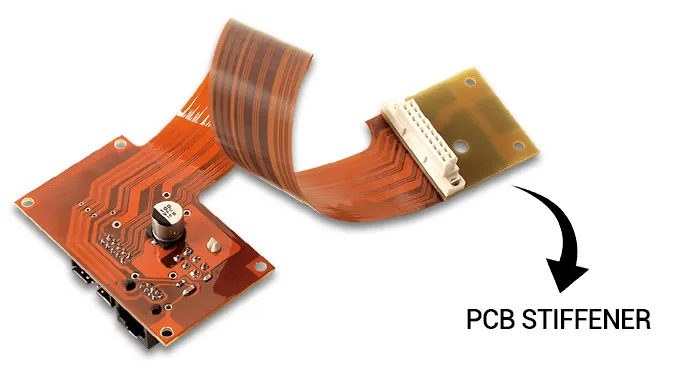
Support structures are essential for maintaining flatness and integrity during flexible PCB panelization. Common approaches include adhesive-backed carrier panels, where the flex array bonds temporarily to a rigid frame, enabling standard rigid-board tooling. Perforated tabs or mouse bites connect individual circuits, distributing stress evenly to prevent localized tearing. These structures must avoid overlapping bend zones or high-density trace areas to preserve functionality. For multilayer flex, embedded stiffeners in rigid-like sections add localized rigidity without compromising overall flexibility.
Framing techniques, such as outer borders with tooling strips, facilitate vacuum fixturing and conveyor transport. Engineers should optimize tab width and spacing based on material thickness, typically 1 to 2 millimeters for tabs to balance strength and ease of removal. In rigid-flex designs, support extends to protecting flex extensions with protective covers or nested layouts. These measures align with IPC-2223 guidelines for sectional design, ensuring reliable transitions between rigid and flexible regions. Proper implementation reduces handling-induced defects by up to several percentage points in yield.
Rigid-Flex PCB Panel Design Best Practices
Rigid-flex PCB panel design integrates rigid multi-layer cores with flexible laminates, requiring layouts that accommodate differential material properties. Panels typically mirror rigid array strategies, with flex sections oriented away from edges to minimize exposure during routing. Symmetric stacking in rigid areas prevents bow and twist, while flex tails use scored lines or tabs for controlled separation. Fiducials straddle rigid-flex boundaries for accurate imaging across the panel. Spacing between boards accounts for flex radius requirements, often 5 to 10 times the material thickness.
Designers prioritize via placement outside bend zones and use fanout patterns to relieve strain in interconnects. Panel borders include break-routing paths that curve around flex areas, avoiding sharp corners that induce microcracks. For assembly, panels incorporate wave-soldering pallets customized for hybrid structures. These practices ensure compatibility with standard equipment while safeguarding flex integrity. Overall, rigid-flex panelization demands iterative simulation of thermal and mechanical stresses to predict performance.
Depaneling Strategies for Rigid-Flex and Flexible PCBs
Depaneling separates individual boards from the panel without damaging delicate flex materials. Mechanical routing suits rigid sections but risks burrs and vibration-induced flex fatigue, so hybrid panels often use it selectively. Laser depaneling offers precision for flexible areas, with wavelengths tuned to ablate copper and polyimide cleanly, minimizing heat-affected zones. Waterjet or UV laser methods further reduce thermal stress, ideal for high-density arrays. Perforated tabs enable manual or pneumatic breakaway for low-volume runs, provided tab design incorporates stress-relief slots.
For rigid-flex PCBs, depaneling sequences rigid areas first, followed by flex tails using non-contact methods. Post-depaneling inspection verifies edge quality per IPC-A-600 criteria, checking for delamination or conductor exposure. Engineers select methods based on volume, material stackup, and tolerance needs, often combining laser for flex and routing for rigid. Clean edges preserve solderability and prevent foreign object debris in assemblies. Effective depaneling maintains panelization benefits through to final product reliability.
Troubleshooting Common Panelization Issues
Warp in flex panels often stems from uneven curing or humidity exposure, addressed by baking panels pre-process and using matched CTE materials. Trace cracking during handling signals inadequate tab support; reinforce with wider perforations or temporary adhesives. Misalignment in rigid-flex arises from flex shrinkage, mitigated by compensation factors in layout software and rigid fiducials. Delamination at interfaces requires adhesive selection per application demands and controlled lamination pressures.
Assembly defects like tombstoning link to panel warpage, resolved via flatness-controlled carriers. Yield data from trials guides iterative refinements, focusing on high-failure zones. Collaborative DFM reviews between design and fab teams catch issues early.
Conclusion
Panelization for flexible and rigid-flex PCBs extends beyond FR-4 simplicity, demanding careful attention to material handling, support structures, and depaneling to achieve efficient production. By integrating best practices like carrier frames, laser separation, and standard-aligned designs, engineers optimize for yield and reliability. Key takeaways include protecting flex areas in layouts, using precise fiducials, and selecting stress-minimizing methods. These strategies enable scalable manufacturing for innovative applications, balancing cost with performance.
FAQs
Q1: What are the main challenges in flexible PCB panelization?
A1: Flexible PCB panelization involves thin substrates prone to warping and tearing during handling. Support structures like tabs and carriers maintain planarity for etching and assembly. Fiducials ensure alignment, while depaneling avoids mechanical stress. Following IPC-6013 helps qualify panels for durability.
Q2: How should rigid-flex PCB panel design account for hybrid materials?
A2: Rigid-flex PCB panel design separates rigid and flex zones, with tabs protecting interconnects. Symmetric rigid stacks prevent twist, and flex tails orient inward. Tooling holes go in rigid sections for stability. This approach supports high-volume handling of flexible materials panelization.
Q3: What support structures are best for flexible PCBs in panels?
A3: Support structures for flexible PCBs include rigid carriers, perforated tabs, and frames for flatness. Adhesives bond arrays temporarily, easing transport. Tabs distribute stress and should be sized to material thickness. These enable standard tooling without damage.
Q4: What depaneling methods work for rigid-flex PCBs?
A4: Depaneling rigid-flex PCBs favors laser for flex precision and routing for rigid efficiency. Non-contact cuts minimize vibration on bends. Post-process checks ensure clean edges. This preserves integrity across the hybrid structure.
References
[IPC-2223E — Sectional Design Standard for Flexible/Rigid-Flexible Printed Boards. IPC, 2021]
[IPC-6013 — Qualification and Performance Specification for Flexible/Rigid-Flexible Printed Boards. IPC, 2014]
[IPC-A-600K — Acceptability of Printed Boards. IPC, 2020]


