ALLPCB


Introduction
In high-power applications such as power supplies, motor drives, and lighting systems, printed circuit boards face significant thermal challenges. Excessive heat generation from components like power transistors and LEDs can lead to performance degradation, reduced lifespan, and outright failure if not addressed properly. Effective PCB thermal management strategies ensure reliable operation by dissipating heat efficiently while maintaining electrical integrity. Engineers must integrate thermal considerations from the initial design phase to optimize board performance under demanding conditions. This article explores proven approaches to handle heat in high-power PCBs, focusing on layout techniques, material choices, and simulation tools tailored for electric engineers.
Why Thermal Management Matters in High-Power PCB Design
Heat buildup in PCBs arises primarily from power dissipation in components and traces, directly impacting reliability and efficiency. Elevated temperatures accelerate material degradation, increase leakage currents, and trigger thermal runaway in semiconductors. In high-power scenarios, such as those exceeding tens of watts, ignoring thermal paths can violate component operating limits and compromise system safety. Proper thermal design aligns with industry expectations for longevity and compliance, preventing costly redesigns or field failures. For electric engineers, mastering these principles means balancing power density with dissipation capabilities to meet application demands.
Fundamental Principles of Heat Transfer in PCBs
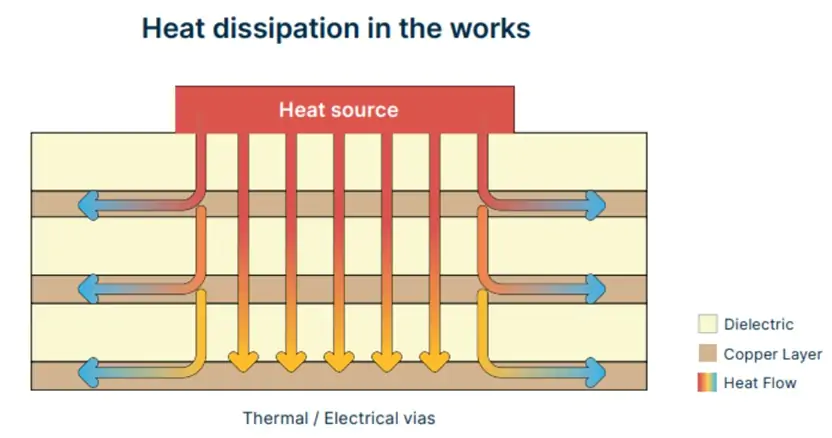
Heat transfer in PCBs occurs through conduction, convection, and radiation, with conduction dominating within the board structure. Components generate heat via Joule heating, where I squared R losses in traces and die junctions raise local temperatures. The thermal resistance, theta JA from junction to ambient, quantifies the heat flow path and guides design decisions. Copper layers act as primary conductors, spreading heat laterally, while vias provide vertical paths between layers. Understanding these mechanisms allows engineers to model hotspots accurately and predict board-level temperatures. Radiation plays a minor role unless surfaces exceed 100 degrees Celsius significantly.
Key Factors Influencing PCB Thermal Performance
Material selection profoundly affects thermal conductivity, with copper foil thickness and dielectric properties determining heat spreading efficiency. Thicker copper, such as 2 oz or more, lowers in-plane resistance but increases weight and cost. Dielectrics with higher glass transition temperatures maintain stability under thermal stress. Board thickness and layer count influence overall impedance to heat flow, requiring trade-offs with signal integrity. Component package types, like QFNs with exposed pads, demand direct thermal connections to inner planes. Environmental factors, including airflow and enclosure constraints, further dictate dissipation potential.
PCB Thermal Management Strategies for Trace and Plane Design
Optimizing trace widths according to current-carrying capacity prevents excessive heating in power paths. Wider traces reduce resistance and temperature rise, ensuring uniform current distribution. Copper pours or planes under high-power components enhance lateral spreading, minimizing hotspots. Filled vias or via stitching arrays bridge layers effectively, creating low-impedance thermal paths. IPC-2221 provides guidelines for these layout elements, emphasizing balanced copper distribution. In practice, engineers iterate designs to achieve theta values compatible with component ratings.
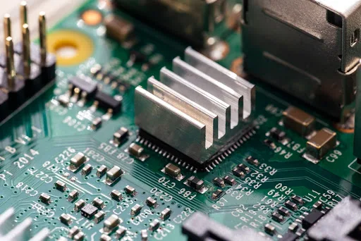
Heat Sink Selection and Integration in PCB Design
Heat sink selection PCB involves matching fin geometry, material, and attachment to the application's thermal load and airflow. Aluminum extrusions offer cost-effective convection surfaces, while forced air improves performance in enclosed systems. The interface between package and sink must minimize contact resistance for optimal conduction. Mechanical clips or adhesives secure sinks without compromising board flexure. Engineers calculate required sink size based on power dissipation and ambient conditions to maintain junction temperatures below limits. Proper orientation aligns with dominant airflow directions over the board.
Role of Thermal Interface Materials in High-Power Applications
Thermal interface material TIM fills microscopic gaps between components and heat sinks, drastically reducing thermal resistance. Gap pads, pastes, or phase-change materials accommodate tolerances and vibrations. Selection criteria include thermal conductivity above 1 W/mK, thickness under 0.2 mm, and compatibility with surface finishes. TIM application requires uniform pressure to avoid voids, which could create hotspots. In stacked assemblies, multiple TIM layers demand careful stacking analysis. This approach proves essential for bridging dissimilar materials in power modules.
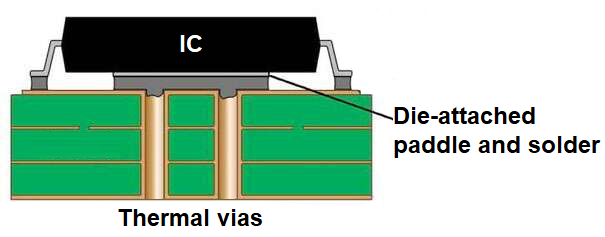
High-Power LED PCB Layout Considerations
High-power LED PCB layout prioritizes direct heat paths from die to board edge or sink. Starburst or radial trace patterns distribute current evenly, minimizing voltage drops and hotspots. Metal-core PCBs with aluminum substrates conduct heat away from clusters efficiently. Thermal vias under LED pads connect to bottom-side planes for external cooling. Copper balance across layers prevents warpage during reflow or operation. Layout symmetry aids uniform dissipation, supporting lumen maintenance over time.

Thermal Vias and Via Field Optimization
Thermal vias consist of plated-through holes arrayed densely under heat sources to transfer flux vertically. Via diameter around 0.3 mm and pitch of 1 mm balance thermal conductance with fabrication yield. Filling vias with conductive epoxy enhances performance in extreme cases. Tentling outer layers protects against solder wicking during assembly. Engineers simulate via field density to optimize without over-perforating the board. This technique multiplies effective conductivity through multilayers.
Advanced Material and Stackup Strategies
Heavy copper multilayers, up to 6 oz outer layers, suit high-current paths with superior spreading. Embedded coins or heat slugs insert high-conductivity islands precisely. Hybrid stackups combine standard FR4 with high-Tg cores for gradient control. Coefficient of thermal expansion matching reduces stress at interfaces. JEDEC JESD51 standards guide package-board thermal characterization, informing stackup choices. These methods scale for power levels above 100 W.
Thermal Simulation in PCB Design
Thermal simulation PCB tools model steady-state and transient behaviors using finite element analysis. Inputs include power maps, material properties, and boundary conditions like convection coefficients. Simulations reveal hotspots early, allowing layout refinements before prototyping. Coupled electro-thermal analysis accounts for resistance changes with temperature. Validation against physical tests refines model accuracy for production. This iterative process cuts development time significantly.
Troubleshooting Common Thermal Issues
Hotspots near power devices often stem from inadequate plane connections or airflow blockage. Measure temperatures with IR cameras or thermocouples to pinpoint issues. Warpage from asymmetric heating requires balanced copper. Delamination risks rise with moisture absorption before thermal cycling. IPC-2152 aids in verifying trace temperatures under load. Systematic checks ensure compliance and reliability.
Best Practices for Implementation
Start with power budgeting to size thermal paths conservatively. Collaborate across design, fabrication, and assembly for feasibility. Prototype with thermocouples for empirical data. Document assumptions in simulation reports. Scale strategies based on validation results.
Conclusion
Mastering PCB thermal management strategies enables robust designs for high-power applications. From layout optimizations and heat sink selection PCB to thermal interface material TIM and simulation, each element contributes to system reliability. High-power LED PCB layout exemplifies integrated approaches. Adhering to standards like IPC-2221 and JEDEC JESD51 ensures industry alignment. Electric engineers benefit from proactive thermal design, yielding longer lifespans and higher efficiencies.
FAQs
Q1: What are the primary PCB thermal management strategies for high-power designs?
A1: PCB thermal management strategies include copper planes for spreading, thermal vias for interlayer transfer, and heat sinks for convection. Material choices like heavy copper enhance conduction. Simulations predict performance pre-fabrication. These methods maintain temperatures within component specs reliably.
Q2: How does heat sink selection PCB impact overall thermal performance?
A2: Heat sink selection PCB depends on power dissipation, airflow, and interface quality. Fin density and base thickness determine theta SA. Proper TIM reduces contact resistance. Matching sink to board footprint avoids mechanical stress. This selection optimizes junction-to-ambient paths effectively.
Q3: Why is thermal simulation PCB essential in high-power applications?
A3: Thermal simulation PCB identifies hotspots and validates strategies early. It models complex interactions like via fields and TIM effects. Engineers refine layouts iteratively. Coupled with standards, it prevents overdesign or failures. This tool streamlines development for demanding power levels.
Q4: What layout tips apply to high-power LED PCB layout?
A4: High-power LED PCB layout uses via arrays under pads and radial traces for even dissipation. Copper balance minimizes warpage. Direct paths to edges or MCPCB cores aid cooling. Symmetry supports uniform performance. These practices sustain LED efficiency long-term.
References
IPC-2221 - Generic Standard on Printed Board Design. IPC.
IPC-2152 - Standard for Determining Current Carrying Capacity in Printed Board Design. IPC.
JEDEC JESD51-2A - Integrated Circuits Thermal Test Method for Low Effective Thermal Conductivity Test Boards. JEDEC.