 ALLPCB


What Is High Density PCB Panelization and Why It Matters
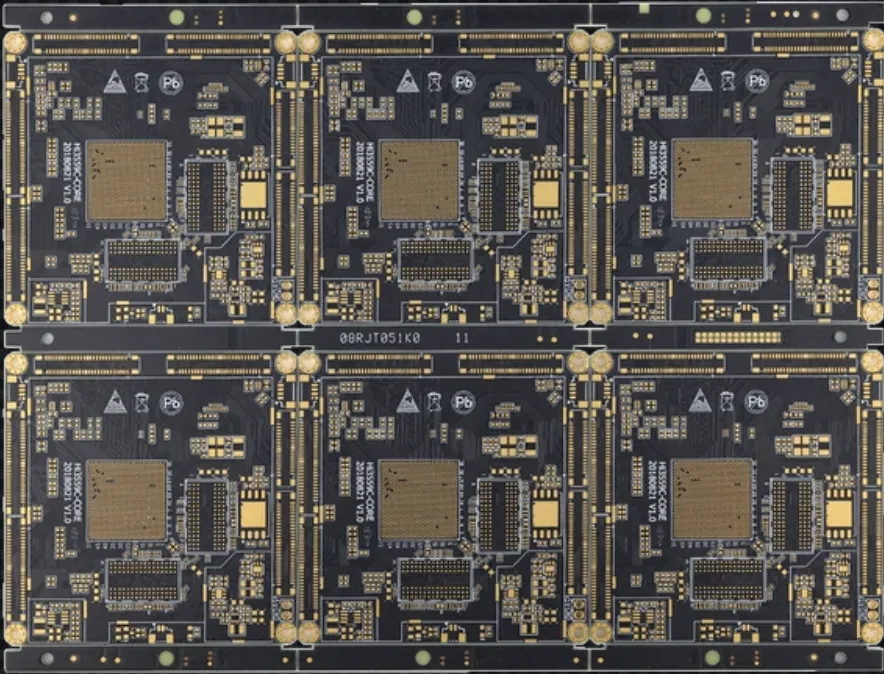
High density PCB panelization refers to the systematic arrangement of densely populated circuit boards onto a standard panel size for collective processing through etching, drilling, plating, and surface-mount assembly. This approach accommodates fine pitch PCB panelization requirements where component leads or ball-grid arrays may have pitches below 0.5 mm. Advanced PCB assembly panel designs incorporate breakaway features and support structures that allow separation without stressing delicate traces or microvias. Industry demand for smaller, more powerful devices drives the need for these methods, as they optimize material use and throughput in high-volume production. Effective panelization also helps control costs by minimizing handling steps and scrap rates associated with individual board processing.
Technical Principles of Panelization for HDI Boards
Panelization for HDI boards begins with layout optimization that positions individual circuits to maximize panel real estate while preserving adequate spacing for routing channels and tooling holes. Engineers calculate panel dimensions based on standard substrate sizes and equipment constraints, ensuring that microvia PCB panel configurations align with drilling and imaging tolerances. Thermal expansion differences between copper layers and dielectric materials must be accounted for to prevent distortion during reflow or lamination cycles. Support structures such as mouse bites or perforated tabs distribute mechanical loads evenly, reducing the risk of cracking in thin cores or build-up layers. These principles integrate with overall board stack-up design to maintain impedance control and signal integrity across the entire panel.
Challenges in Fine Pitch and Microvia Panelization
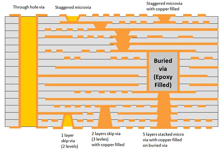
Fine pitch components and microvias introduce specific challenges during panelization because small feature sizes amplify the effects of mechanical stress and thermal gradients. Warpage can occur when copper distribution is uneven across the panel, leading to misalignment during solder paste printing or component placement. Microvia structures, often stacked or staggered, require careful placement away from panel edges and break lines to avoid delamination or barrel cracking. High density PCB panelization must also address vibration and flexing during depanelization, which can damage fine traces or solder joints on adjacent boards. Thermal management becomes critical in dense layouts where heat buildup during assembly may exceed material glass-transition temperatures if panel support is inadequate.
Best Practices and Advanced Techniques
Design teams begin by selecting panelization methods suited to board thickness and component density, such as V-scoring for straight-line separation or tab routing for irregular shapes. Advanced PCB assembly panel strategies include adding sacrificial borders or rails that provide rigidity during handling and are removed in the final step. For microvia PCB panel designs, engineers specify symmetrical copper balancing and controlled-impedance routing to minimize warpage, often verified through simulation before fabrication. Depanelization parameters, including feed rates and tool selection, are optimized to limit mechanical shock to fine-pitch areas. Collaboration between design and manufacturing teams ensures that panelization features comply with assembly equipment capabilities and reduce the need for manual intervention.
Quality Control Considerations
Quality control in high density PCB panelization involves dimensional verification of panel features, including hole positions, tab widths, and scoring depths, to ensure compatibility with downstream processes. Visual and automated optical inspection checks for surface defects, while X-ray imaging confirms microvia integrity in dense regions. Thermal cycling and mechanical stress tests simulate assembly conditions to validate panel stability. These steps help maintain consistency across production runs and support traceability requirements in regulated industries.
Conclusion
Advanced panelization techniques enable reliable production of high-density boards by addressing the unique demands of fine features and microvias. Through careful layout, material balancing, and process optimization, manufacturers achieve higher yields and improved assembly performance. Adherence to established engineering practices ensures that panels withstand the rigors of modern fabrication and assembly environments.
FAQs
Q1: What factors influence the choice of panel size for high density PCB panelization?
A1: Panel size selection depends on substrate availability, equipment capacity, and the need to accommodate fine pitch components and microvias while maintaining mechanical stability. Engineers evaluate copper distribution and thermal properties to minimize warpage across the panel. Standard sizes are often chosen to align with industry equipment, balancing material utilization against handling requirements.
Q2: How does fine pitch PCB panelization differ from standard panelization?
A2: Fine pitch PCB panelization requires tighter tolerances on breakaway features and greater attention to stress distribution near small-pitch components. Support structures must avoid proximity to microvias or dense routing to prevent damage during separation. Thermal and mechanical simulations are typically used to validate designs before production.
Q3: What role do microvias play in determining advanced PCB assembly panel layouts?
A3: Microvias influence panel layouts by requiring precise alignment and sufficient clearance from edges or break lines to maintain structural integrity. Their placement affects copper balancing and thermal expansion behavior across the panel. Proper positioning supports reliable plating and reduces the risk of defects during assembly.
Q4: Why is warpage control important in microvia PCB panel processing?
A4: Warpage control prevents misalignment during solder paste application and component placement on high-density boards. Uneven expansion can stress microvias and fine traces, leading to reliability issues after reflow. Balanced designs and verification testing help maintain flatness throughout manufacturing.


