 ALLPCB


What Is Advanced Outer Layer Microvia Design and Why It Matters
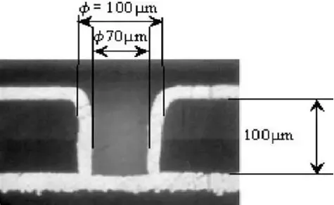
Advanced outer layer microvia design refers to the precise engineering of laser-drilled vias that connect the outermost copper layers to inner layers in HDI PCBs. These vias typically range from 0.05 mm to 0.15 mm in diameter and enable higher interconnect density than traditional through-hole vias. In HDI PCB microvia design, designers must balance electrical requirements, thermal considerations, and manufacturing constraints to achieve reliable performance.
The approach matters because it allows electronic devices to shrink in size while increasing functionality. Consumer electronics, automotive control modules, and medical instruments all benefit from the space savings and improved signal paths that result from optimized microvia layouts. Without careful design, issues such as plating voids or mechanical stress can lead to field failures.
Technical Principles of Laser Drilled Vias and Microvia Configurations
Laser drilled vias form the foundation of most outer layer microvia structures. A focused laser ablates the dielectric material to create a precise hole that stops at the target copper layer. This process produces cleaner walls than mechanical drilling and supports the small diameters required for high-density routing.
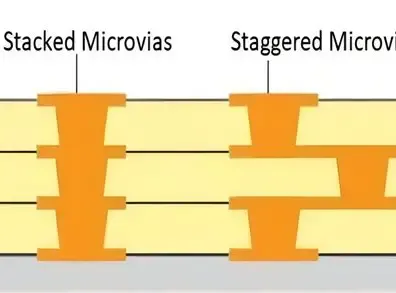
Stacked microvias place multiple vias directly on top of one another to span several layers. This configuration minimizes the horizontal space consumed by via pads but concentrates mechanical stress at the interfaces. Staggered microvias offset each via slightly, distributing stress across a broader area and often improving long-term reliability under thermal cycling.
Microvia filling completes the structure by depositing copper or conductive material inside the hole. Filled vias provide a planar surface for subsequent lamination or component attachment and enhance thermal conductivity. Unfilled or partially filled vias may suffice for low-current signals but require careful evaluation of current-carrying capacity and void formation risks.
Aspect ratio remains a critical parameter. Ratios exceeding 1:1 demand tighter process controls during drilling and plating to ensure complete copper coverage. Designers evaluate these ratios early in the layout phase to avoid manufacturing defects.
Practical Solutions and Best Practices for Reliable HDI PCB Microvia Design
Design rules should specify minimum land diameters, annular ring requirements, and clearance distances based on the chosen microvia type. Stacked configurations often need additional copper thickness on target pads to accommodate cumulative plating stress. Staggered layouts benefit from optimized pad offsets that maintain signal integrity while easing registration tolerances during fabrication.
Thermal management considerations include via placement relative to heat-generating components. Placing microvias under or near power devices can improve heat dissipation when the vias are properly filled. Engineers also evaluate coefficient of thermal expansion mismatch between the dielectric and copper to reduce the risk of barrel cracking.
Process validation through test coupons helps confirm that the chosen microvia parameters meet performance expectations. Coupon designs replicate the production stackup and via configurations, allowing measurement of plating thickness, void content, and mechanical strength before full production begins.
IPC-6012E provides qualification and performance criteria that guide acceptance of HDI constructions containing microvias. Designers reference these criteria when establishing acceptance limits for via fill quality and structural integrity.

Manufacturing and Quality Considerations
Fabrication teams must maintain tight control over laser parameters, including pulse energy and beam focus, to achieve consistent hole geometry. Variations in dielectric thickness or resin content can affect drilling depth and wall quality. Close collaboration between design and manufacturing ensures that layout files include all necessary data for accurate via formation.
Post-drilling cleaning removes debris that could interfere with plating adhesion. Subsequent copper deposition must achieve uniform thickness along the via walls and on the target pad. Filled microvias undergo additional planarization steps to restore a smooth surface for the next lamination cycle.
Quality control procedures include cross-section analysis and electrical testing to detect discontinuities or excessive resistance. These checks verify that the microvia structures perform as intended under both direct current and high-frequency conditions.
Conclusion
Advanced outer layer microvia design enables the compact, high-performance PCBs required by today’s electronic systems. Careful selection between stacked and staggered configurations, combined with appropriate filling methods, supports both density and reliability goals. Adherence to established industry practices helps engineers deliver designs that meet electrical, thermal, and mechanical requirements throughout the product lifecycle.
FAQs
Q1: What distinguishes stacked microvias from staggered microvias in HDI PCB microvia design?
A1: Stacked microvias align vertically through multiple layers to conserve horizontal space, while staggered microvias offset each via to distribute mechanical stress. Both approaches support high-density routing, but staggered layouts often provide better long-term reliability under thermal cycling. Designers select the configuration based on board thickness, layer count, and expected operating conditions.
Q2: How does laser drilled via technology support advanced outer layer microvia design?
A2: Laser drilling creates small-diameter holes with high precision and minimal damage to surrounding material. This capability allows outer layer microvias to connect fine-pitch components without consuming excessive board area. The process also enables consistent via formation across large panel sizes when process parameters remain tightly controlled.
Q3: Why is microvia filling important in HDI PCB constructions?
A3: Filling microvias with copper or conductive material creates a solid, planar structure that supports subsequent lamination and component attachment. Filled vias improve thermal transfer and current-carrying capacity compared with unfilled holes. Proper filling also reduces the risk of voids that could compromise electrical continuity or mechanical strength.
Q4: What design factors influence the choice between stacked and staggered microvias?
A4: Key factors include overall board thickness, target aspect ratio, thermal expansion characteristics of the materials, and the mechanical stresses expected during assembly and operation. Stacked configurations suit applications where routing density is paramount, whereas staggered designs often provide greater margin for reliability in demanding environments.
References
IPC-6012E — Qualification and Performance Specification for Rigid Printed Boards. IPC, 2017
IPC-A-600K — Acceptability of Printed Boards. IPC, 2020
IPC-4761 — Design Guide for Protection of Printed Board Via Structures. IPC, 2006





