ALLPCB


Overview
This article reviews circuit protection techniques and PCB layout strategies to protect wearable augmented reality (AR) devices and their users. Applying these five recommendations early in the design process helps circuit designers improve the performance, safety, and reliability of wearable designs and supports a more robust IoT ecosystem.
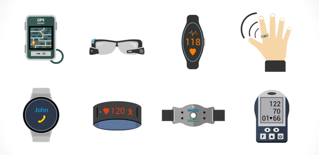
New display technologies will allow virtual content to be layered over the real world through lenses, creating augmented reality. Examples include turn-by-turn navigation in AR glasses, face recognition, fitness tracking, first-person photos and video, and health and travel applications.
As chipsets used in wearables become smaller, the area required for integrated circuits and the footprint of circuit protection devices must shrink accordingly.
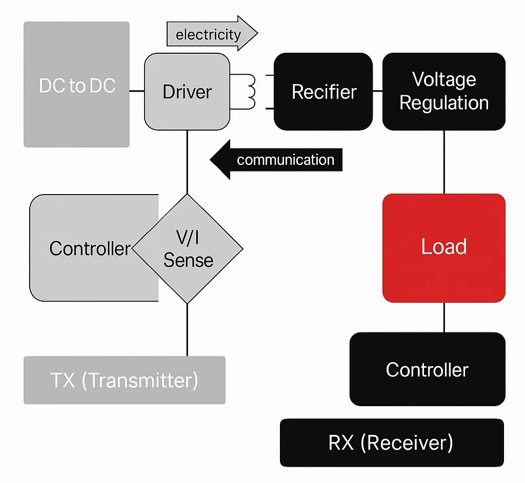
ESD considerations for wearables: TVS diode selection and placement
1. Small package sizes
Modern ESD diodes in compact packages provide performance advantages for AR applications. The guidance below helps engineers select and configure ESD diodes to optimize future circuit designs.
2. Choose unidirectional or bidirectional diodes
ESD diodes are available in unidirectional and bidirectional configurations. Unidirectional diodes are typically used in DC circuits, including buttons, keyboards, and digital lines. Bidirectional diodes are used in AC circuits where signal swings can go below -0.7 V; examples include audio, analog video, legacy data ports, and RF interfaces.
Prefer unidirectional diodes when possible to improve performance against negative-voltage ESD strikes. During such transients, the clamp voltage is based on the diode's forward bias, typically under 1.0 V. In contrast, a bidirectional diode clamps on its reverse breakdown, which is higher than the forward-bias voltage of a unidirectional device. Therefore, a unidirectional configuration can significantly reduce stress on the system during negative transients.
3. Determine diode placement
Most circuits do not require a board-level ESD diode on every IC pin. Designers should identify pins that may be exposed to user-generated ESD events. Any communication or control line that users can touch can become a path for ESD into the IC. Typical circuits include USB, audio, buttons, switches, antennas, and other data buses. Adding discrete protection devices consumes PCB area, so minimizing footprint to 0201 or 01005 is important. Some manufacturers offer space-saving multichannel arrays for certain wearable applications. It is generally recommended to place ESD devices as close as possible to the ESD entry point, typically at connectors or I/O ports.
4. Route the ESD path carefully
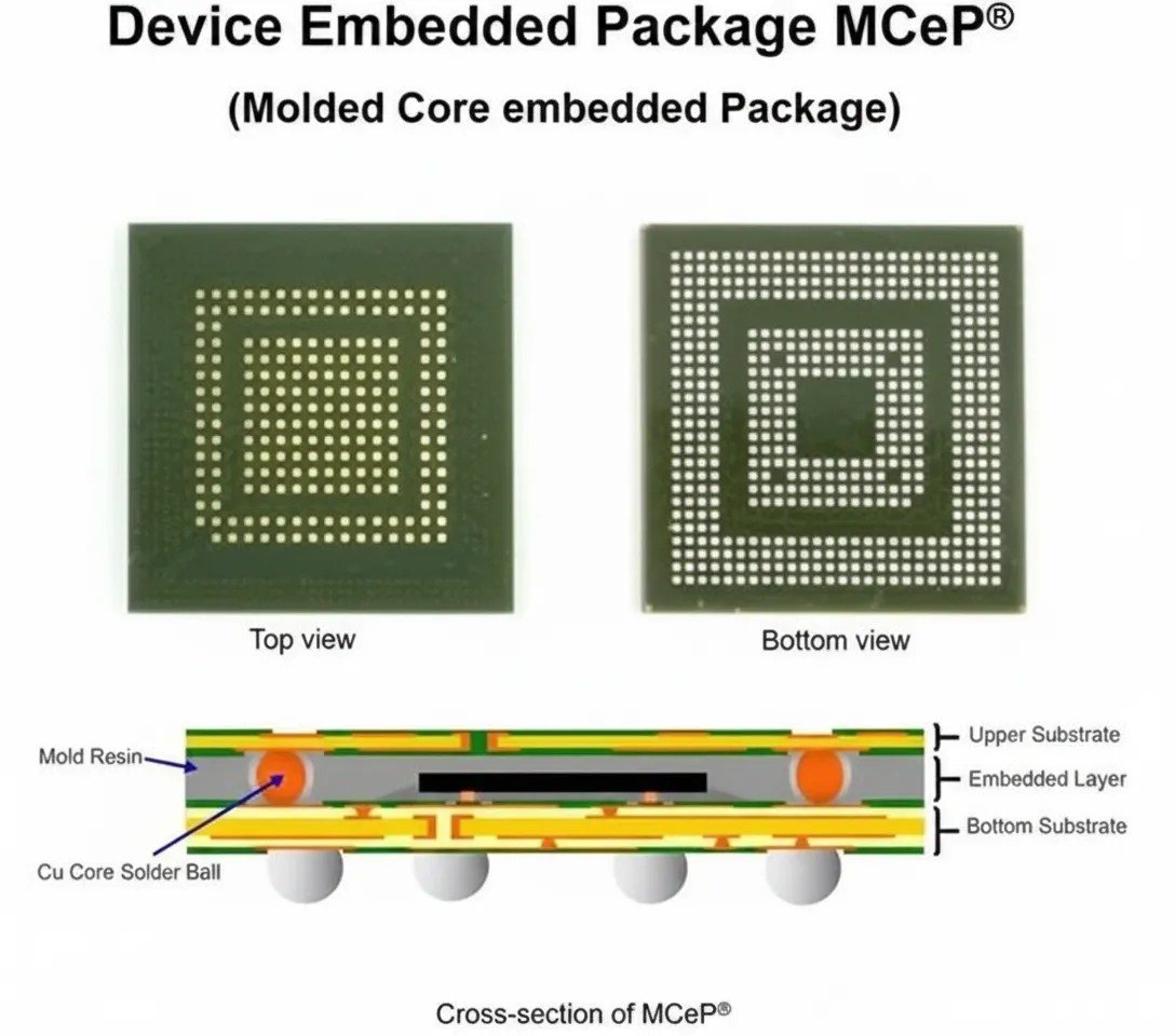
To protect IC pins with ESD diodes, several PCB routing factors are critical for the path from I/O to ground. Unlike lightning transients, ESD does not deliver large currents for an extended period. To handle electrostatic discharge effectively, the charge arriving at the protected circuit must be transferred to the ESD device as quickly as possible. The trace length from the I/O to the ESD device and from the ESD device to the power-ground reference is the most important factor, not trace width. Keep these traces as short as possible to limit parasitic inductance. That inductance can cause an inductive overshoot, producing a transient voltage spike; with sufficiently long traces, that pulse voltage can reach hundreds of volts. New package developments, including micro DFN and wafer-level chip-scale packaging, are well suited for data channels and can eliminate long traces that would otherwise require additional ESD protection.
5. Understand HBM, MM, and CDM definitions
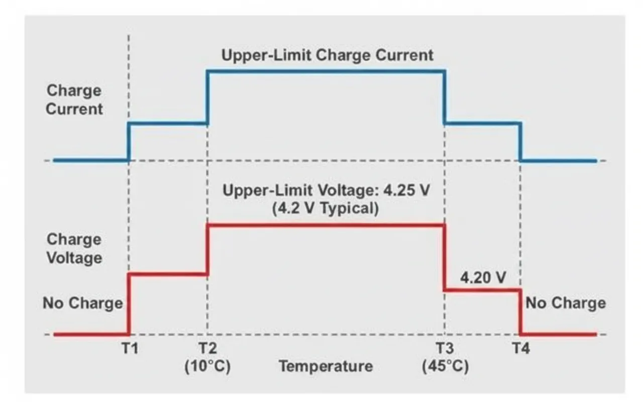
HBM (human body model), MM (machine model), and CDM (charged-device model) are test models used to characterize the ESD robustness of ICs used in portable or wearable devices, including processors, memory, and ASICs. Semiconductor vendors use these tests to ensure robustness during manufacturing. The trend toward lower test-voltage levels can reduce chip area. In addition, many electronics manufacturers implement ESD controls and countermeasures during assembly. If ESD protection is only implemented during assembly, devices remain vulnerable to ESD damage in consumer environments. Without adequate built-in ESD protection, devices can experience gradual degradation or catastrophic failure in the field. Designers must select board-level devices robust enough to withstand high electrical stress while meeting the bandwidth and performance requirements of the final product.
Key parameters when evaluating ESD protection devices
- Dynamic resistance: Defines the diode's resistance while clamping a transient from the source to the energy sink. This value indicates how quickly a diode can clamp an ESD pulse and divert it to ground. A more vertical I-V or TLP curve indicates a more efficient avalanche diode and lower dynamic resistance.
- IEC 61000-4-2 rating: This tested and verified rating reflects how repeatedly an ESD diode can withstand discharges without degrading DC performance. For this parameter, higher values are generally better. Some ESD diodes reach 20 kV or 30 kV under contact discharge conditions, exceeding the nominal 8 kV air discharge industry reference.
- DC performance: Important DC-related considerations when protecting a circuit include surge withstand (8/20 μs), parasitic capacitance, parasitic inductance, and nominal and maximum leakage current.
Space-saving discrete TVS arrays in low capacitance, bidirectional configurations provide symmetric ESD protection for high-speed data lines when AC signals are present. They are used in consumer products such as fitness bands, smartwatches, smartphones, tablets, and e-readers.