ALLPCB


Overview
To support efficient information transfer and communication, 5G and 6G networks require more antennas, larger bandwidth, and higher base station density. Demand for radio frequency (RF) electronic components will increase substantially in the coming years. For example, the number of global 5G base stations is projected to grow significantly by 2025. Alongside explosive growth in RF devices, especially mobile terminals, electromagnetic pollution is an urgent challenge.
Historically, conductive materials for RF devices and electromagnetic interference (EMI) shielding have been metal-based. However, increasing requirements for flexibility, high integration, lightweight design, manufacturability, and operation at higher frequencies make metal-based structures less suitable for future RF devices. In addition, the growing volume of electronic products raises concerns about electronic waste and environmental impact, making sustainability an important consideration for next-generation consumer electronics.
Graphene Assembled Film (GAF) for RF
Since early development, conductive materials in wireless communication and EMI shielding have been primarily metal structures. The team led by He Daping at Wuhan University of Technology proposed a graphene assembled film (GAF) as a potential replacement for copper in such practical electronic products.
Advantages of GAF
Corrosion resistance of GAF-based antennas
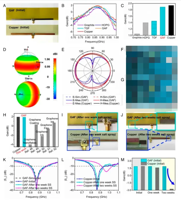
Figure 1: GAF used as a dipole antenna and its corrosion resistance. (A) Digital photos of GAF and copper dipole antennas. (B) Measured gain across bandwidths for antennas made of different materials. (C) Gain of different-material antennas at 865 MHz. (D) 3D radiation pattern simulation of the GAF antenna. (E) E-plane and H-plane radiation patterns of GAF and copper antennas. (F and G) Measurement environments for E-plane and H-plane patterns, respectively. (H) Comparison of dipole antenna gain from literature with results in this work. (J) Digital photos of GAF and copper dipole antennas after 1 week and 2 weeks of salt spray exposure. (K) Measured and simulated |S11| of the GAF antenna initially, after 1 week, and after 2 weeks of salt spray. (L) Measured |S11| of the copper antenna initially, after 1 week, and after 2 weeks of salt spray. (M) Measured gain of GAF and copper antennas at 865 MHz under initial, 1 week, and 2 week salt spray conditions.
After two weeks of salt spray testing, electrical performance metrics such as gain and reflection coefficient remained unchanged for GAF, whereas the copper antenna was corroded and damaged.
Wider operational bandwidth
GAF ultra-wideband antennas cover 3.7 GHz to 67 GHz, providing a bandwidth of 63.3 GHz, which is about 110% wider than comparable copper-foil antennas. Compared with copper antennas, GAF-based 5G antenna arrays exhibit broader bandwidth and lower sidelobe levels. The research also shows that GAF-based metamaterial frequency-selective surfaces (FSS) act as flexible frequency-selective sheets with promising frequency selection characteristics and angular stability.
Higher conductivity and mechanical robustness
GAF achieves an electrical conductivity up to 2.58 × 10^6 S/m. After 200,000 bending cycles with a bend radius of 1.5 mm, the graphene assembled film maintained high flexibility and conductivity without structural damage. To assess performance in 5G and flexible electronics scenarios, the team demonstrated flexible GAF-based coplanar waveguide transmission lines and resonators, showing stable performance under various twisting conditions. GAF-based dipole antennas offer good reflection coefficients and high gain comparable to copper antennas.
Superior electromagnetic shielding
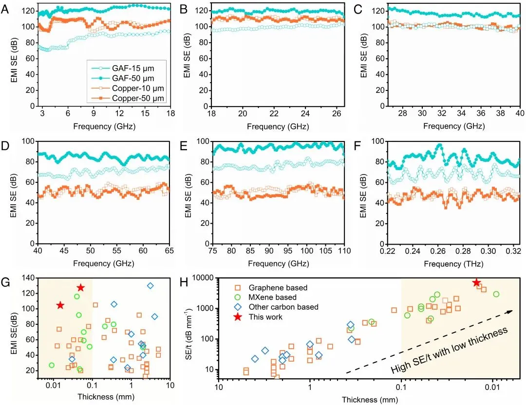
Figure 2: GAF applied to EMI protection. (A–F) EMI shielding effectiveness (SE) for 15 μm and 50 μm GAF and 10 μm and 50 μm copper across 2.6 GHz to 0.32 THz: (A) 2.6 to 18 GHz (rectangular waveguide), (B) 18 to 26.5 GHz (rectangular waveguide), (C) 26.5 to 40 GHz (rectangular waveguide), (D) 40 to 67 GHz (free-space method), (E) 75 to 110 GHz (free-space method), and (F) 0.22 to 0.3235 THz (free-space method).
GAF's EMI shielding effectiveness also outperforms copper, reaching up to 127 dB across 2.6 GHz to 0.32 THz. Normalized by thickness, SE reaches 6,966 dB/mm, exceeding copper of equivalent thickness.
Beyond full shielding, selective shielding of specific frequency bands is often necessary to preserve communication in other bands. As a metamaterial, frequency-selective surfaces (FSS) consist of periodically arranged unit structures that can selectively absorb, reflect, or transmit electromagnetic waves. GAF-based FSS maintained stable frequency-selection performance under bending angles of 0° to 40° and showed good frequency-selective behavior for incident angles up to ±30°, indicating high angular stability.
GAF Manufacturing
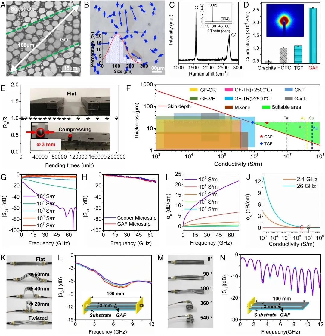
Figure 3: GAF characterization. (A) Typical TEM image of large GO sheets with lateral size around 108 μm. (B) Optical microscope image of LGO sheets prepared by drop-casting LGO solution onto SiO2, with inset showing lateral size distribution statistics. (C) XRD and Raman spectra of GAF. (D) Summary of electrical conductivity for GAF, graphite, highly oriented pyrolytic graphite (HOPG), and typical flake-size GO assembled films (TGF), with inset SAXS patterns. (E) Resistance change of GAF after 200,000 repeated bending tests, demonstrating durable flexibility and stability. (F) Skin depth at 860 MHz versus conductive layer thickness for materials prepared by chemical reduction, vacuum filtration, thermal reduction of GO films, graphene ink, carbon nanotubes (CNT), and MXene. (G and H) Simulation and measurement of the transmission coefficient of multilayer transmission lines (MTL). (I and J) Conductor loss under different frequencies and conductivities. (K) Flexible GAF FCPW transmission lines bent to diameters of 60 mm, 40 mm, and 20 mm and twisted 180°. (L) Transmission coefficient of FCPW TL from 10 MHz to 40 GHz under different states. (M) Flexible GAF λ/4 short-circuit resonators under twist conditions: untwisted, 90°, 180°, 360°, and 540°. (N) Reflection coefficient results of the resonators from 10 MHz to 12 GHz under different twist conditions.
Two main approaches were used to achieve high conductivity in graphene laminated films. First, the team maximized graphene microcrystal size to reduce contact resistance. Second, they implemented a secondary annealing process and specialized assembly techniques to laminate these graphene microcrystals into continuous, defect-free films.
Graphene oxide (GO) was prepared using an improved Hummers method. Large GO (LGO) fractions were separated and collected as precursors for film fabrication. After seven repeated centrifugation steps, LGO was isolated from a 3 wt.% GO suspension by collecting the bottom 30% of GO each time. Optical microscopy statistics show that 74% of LGO has lateral size >75 μm and 54% >100 μm. Typical sheet-size GO (TGO) was also synthesized for comparison. LGO assembled films were prepared by roll transfer coating of premeasured LGO hydrogel onto self-release substrates such as PET film.
The LGO hydrogel on the substrate was dried at 70 to 80 °C. A soft, deep-brown freestanding paper-like GO film (LGO film) could then be peeled from the PET substrate. The anisotropic liquid-crystal behavior of the LGO hydrogel produced prealigned structures after force-directed roll transfer.
The highly ordered laminate was converted into meter-scale graphitic films via high-temperature graphitization. LGO films were thermally annealed between graphite plates in an Ar atmosphere at 1,300 °C for 2 hours and at 2,850 °C for 1 hour for reduction and graphitization. Large crystalline graphite domains in GAF formed by merging neighboring reduced LGO sheets.
After initial high-temperature annealing, the film became fully graphitized, allowing defect-free graphene nanoplatelets to lay flat via large-area plane contacts. Subsequent rolling compression at 300 MPa eliminated interlayer gaps and contact resistance, improving conductivity and providing superior flexibility.
Following rolling compression, a secondary annealing at 2,850 °C in Ar was used to repair structural damage from rolling and further increase conductivity. The same process applied to TGO produced TGF.
Conclusion
The team led by He Daping demonstrated a lightweight, flexible, mechanically durable, chemically stable, and highly conductive GAF structure suitable for multi-band 5G wireless components and electromagnetic protection, addressing several limitations of copper-based electronics. GAF-based 5G devices can be designed in complex patterns and integrated into communication systems to provide advanced functionality across microwave communication bands.
GAF also shows excellent electromagnetic shielding in microwave and terahertz bands and can be patterned as metamaterials for selective electromagnetic shielding. The research indicates that highly conductive graphene films can serve as a full-featured, more sustainable alternative in RF applications, supporting current and next-generation flexible electronics, wireless communication equipment, and EMI shielding solutions.