 ALLPCB


Aviation and aerospace systems demand printed circuit boards that perform without failure under extreme conditions. Engineers designing aviation PCB solutions must focus on reliability from the initial concept through final deployment. This emphasis stems from the critical roles these boards play in flight controls, navigation, communication, and power management systems. Failures in such environments can lead to significant operational disruptions or safety concerns. The following discussion outlines three essential rules that guide effective aviation PCB design and production.
Why Aviation PCB Reliability Matters in Modern Aerospace Applications
Aviation PCB design requires boards capable of withstanding continuous vibration, wide temperature swings, and potential exposure to radiation or electromagnetic interference. These conditions differ markedly from those in consumer or industrial electronics. Aerospace PCB reliability directly influences mission success in both manned aircraft and unmanned systems. Procurement teams and designers therefore evaluate every material choice and manufacturing step against long-term performance needs. Standards organizations have developed specific guidelines to address these unique demands.
Rule 1: Adhere to IPC Class 3 Requirements for High-Reliability Boards
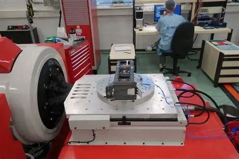
IPC Class 3 PCB specifications define the highest level of acceptance criteria for printed boards used in life-support or mission-critical applications. This classification demands tighter tolerances on conductor spacing, hole plating quality, and laminate integrity compared with lower classes. Manufacturers following these criteria perform extensive visual and electrical inspections to identify even minor anomalies. The result is boards with enhanced resistance to thermal cycling and mechanical stress. Designers benefit from specifying IPC Class 3 early because it shapes layout decisions such as trace widths and via structures.
Rule 2: Implement AS9100D-Aligned Quality Management Throughout the Supply Chain
AS9100D certification PCB processes integrate additional aerospace-specific requirements onto established quality frameworks. These include rigorous configuration management, risk assessment at every stage, and full traceability of materials and processes. Teams maintain detailed records that allow any board to be traced back to its raw materials and production lot. Such practices reduce the likelihood of latent defects emerging during service. Regular internal audits and supplier evaluations reinforce consistent output across multiple production runs.
Rule 3: Design for Environmental Extremes Encountered in Space Travel, Satellites, and National Defense
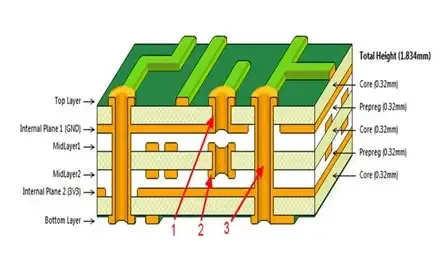
PCB for space travel and PCB for satellites must tolerate vacuum conditions, intense radiation, and rapid temperature changes without performance degradation. Similar considerations apply to PCB for national defense platforms operating in harsh field environments. Engineers incorporate features such as conformal coatings, robust thermal vias, and radiation-tolerant component selections. Layout strategies also address vibration damping and electromagnetic shielding. These choices are validated through environmental stress screening that simulates operational profiles.
Practical Design and Manufacturing Best Practices
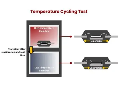
Engineers begin by selecting base materials with appropriate glass transition temperatures and low coefficients of thermal expansion. They then apply design rules that minimize stress concentrations around plated through-holes and surface-mount pads. During fabrication, process controls focus on consistent copper plating thickness and dielectric layer uniformity. Assembly teams use controlled soldering profiles and inspect joints against established acceptability criteria. Post-assembly testing includes burn-in, vibration, and thermal shock sequences tailored to the intended application profile. Documentation of every step supports ongoing reliability monitoring once units enter service.
Conclusion
Reliability in aviation PCB design rests on three interconnected rules: adherence to IPC Class 3 criteria, alignment with AS9100D quality systems, and proactive design for extreme environments. These principles guide decisions from schematic capture through final acceptance testing. When followed consistently, they produce boards that meet the stringent demands of aerospace, satellite, and defense programs. Continued attention to these areas helps engineering teams deliver solutions that perform reliably over extended operational lifetimes.
FAQs
Q1: What distinguishes aviation PCB design from standard commercial board design?
A1: Aviation PCB design incorporates stricter material selections, tighter manufacturing tolerances, and additional environmental testing to ensure performance under vibration, temperature extremes, and electromagnetic stress. These measures support long-term reliability in flight-critical systems.
Q2: How does AS9100D certification PCB improve traceability compared with general quality standards?
A2: AS9100D certification PCB processes add aerospace-specific requirements for configuration control, risk management, and material traceability that extend beyond basic quality management frameworks. This enables complete tracking from raw materials to finished assemblies.
Q3: Why is IPC Class 3 PCB preferred for PCB for space travel and satellites?
A3: IPC Class 3 PCB criteria enforce the most rigorous acceptance standards for defects, plating quality, and structural integrity. These requirements help boards withstand radiation, thermal cycling, and mechanical loads typical in orbital and deep-space missions.
Q4: What role does environmental testing play in ensuring aerospace PCB reliability?
A4: Environmental testing subjects boards to simulated vibration, thermal cycling, and other stressors to identify weaknesses before deployment. Results guide design refinements and confirm that assemblies will maintain function throughout their service life.





