 ALLPCB


If you're facing challenges with PCB direct imaging, you're not alone. Many engineers and manufacturers encounter issues like misalignment, inconsistent exposure, or defects during the Laser Direct Imaging (LDI) process. In this comprehensive guide, we'll dive into the most common problems with PCB direct imaging and provide practical solutions to help you achieve flawless results. Whether you're troubleshooting LDI process problems or looking to prevent direct imaging defects, this post covers everything you need to know about maintaining quality in PCB manufacturing.
What is PCB Direct Imaging and Why Does It Matter?
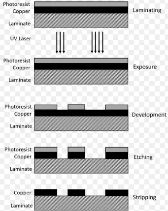
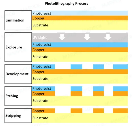
PCB direct imaging, often referred to as Laser Direct Imaging (LDI), is a cutting-edge technology used in printed circuit board manufacturing. Unlike traditional photolithography, which relies on film masks, LDI uses a laser to directly transfer circuit patterns onto the photoresist layer of a PCB. This method offers higher precision, faster production times, and the ability to handle complex designs with fine traces, often down to line widths of 25 micrometers or less.
However, with such precision comes the potential for errors if the process isn't optimized. Direct imaging defects can lead to costly rework, delays, and even product failures. Understanding how to troubleshoot PCB direct imaging issues is crucial for maintaining efficiency and quality in manufacturing.
Common Issues in PCB Direct Imaging
Let’s explore the most frequent problems encountered during the LDI process. By identifying these issues early, you can take steps to minimize their impact on your production line.
1. Misalignment of Circuit Patterns
One of the most common PCB manufacturing errors in direct imaging is misalignment. This happens when the laser doesn't accurately position the circuit pattern on the board, resulting in shifted traces or pads. Misalignment can cause short circuits or open connections, especially in high-density interconnect (HDI) designs where tolerances are tight, often below 50 micrometers.
Causes:
- Incorrect calibration of the LDI machine.
- Mechanical vibrations or instability during imaging.
- Improper panel placement or fixturing.
Solutions:
- Regularly calibrate the LDI equipment to ensure precise laser alignment. Check calibration at least once per shift or after every 100 panels processed.
- Secure the machine on a stable, vibration-free surface and inspect for any loose components.
- Use high-quality fixtures to hold panels in place during imaging, ensuring repeatability within 10 micrometers.
2. Inconsistent Exposure Levels
Inconsistent exposure occurs when the laser energy varies across the board, leading to uneven development of the photoresist. This can result in overexposed areas where traces are too thin (under 20 micrometers) or underexposed areas where traces remain incomplete.
Causes:
- Fluctuations in laser power output, often due to aging components.
- Dust or debris on the laser lens, scattering the beam.
- Variations in photoresist thickness, sometimes differing by 5-10 micrometers across a panel.
Solutions:
- Monitor laser power output using built-in diagnostics and replace components when power drops below 90% of the rated value.
- Clean the laser lens regularly with a non-abrasive cloth and approved cleaning solution to prevent beam distortion.
- Ensure uniform photoresist application by using automated coating machines and verifying thickness with a gauge.
3. Direct Imaging Defects Like Spots or Scratches
Spots, scratches, or other surface defects on the PCB during imaging can ruin an entire batch. These direct imaging defects often appear as unintended marks or breaks in the circuit pattern, leading to functional failures.
Causes:
- Contamination on the PCB surface, such as dust particles or fingerprints.
- Damaged or dirty protective layers on the board.
- Laser beam irregularities caused by worn-out optics.
Solutions:
- Handle PCBs in a cleanroom environment with a minimum ISO Class 7 rating to reduce contamination risks.
- Inspect and replace protective films before imaging to avoid transferring defects to the photoresist.
- Schedule regular maintenance for the LDI system, replacing optics when they show signs of wear, typically after 10,000 hours of operation.
4. Software and Data Transfer Errors
The LDI process relies heavily on digital design files to guide the laser. Errors in data transfer or software glitches can lead to incorrect patterns being imaged, a critical PCB manufacturing error that’s often overlooked.
Causes:
- Corrupted design files or incompatible file formats.
- Software bugs or outdated firmware in the LDI system.
- Communication failures between the design software and imaging hardware.
Solutions:
- Validate design files using pre-imaging software checks to ensure compatibility and integrity before loading them into the LDI system.
- Keep LDI system software and firmware updated to the latest versions to avoid bugs and improve performance.
- Use reliable, high-speed data transfer protocols to prevent interruptions during file loading.
Preventing LDI Process Problems Through Maintenance
Direct imaging maintenance is key to avoiding many of the issues discussed above. A well-maintained LDI system not only reduces defects but also extends the lifespan of the equipment, saving costs in the long run. Here are essential maintenance tips for preventing LDI process problems.
1. Routine Cleaning of Equipment
Dust and debris can accumulate on critical components like the laser lens, mirrors, and imaging bed, leading to reduced accuracy. Clean these parts weekly using manufacturer-recommended solutions and tools to maintain imaging quality.
2. Regular Calibration Checks
Calibration drift can occur over time, especially in high-volume production environments. Schedule calibration checks at least monthly or after every 500 imaging cycles to ensure the laser aligns within a tolerance of 5 micrometers.
3. Monitoring Environmental Conditions
Temperature and humidity fluctuations can affect the LDI process. Maintain a controlled environment with temperatures between 20-25°C and humidity levels of 40-60% to prevent material expansion or contraction, which can skew imaging accuracy by up to 10 micrometers per degree of change.
4. Updating System Software
Software updates often include fixes for known issues and performance enhancements. Check for updates quarterly and apply them during scheduled downtime to avoid disrupting production.
Advanced Tips for Optimizing PCB Direct Imaging
Beyond troubleshooting and maintenance, there are ways to optimize the LDI process for even better results. These advanced strategies can help reduce PCB manufacturing errors and improve overall efficiency.
1. Use High-Quality Photoresist Materials
Not all photoresists are created equal. Choose materials with consistent sensitivity to the laser wavelength used in your LDI system, typically around 355-405 nanometers for UV lasers. High-quality photoresists can reduce exposure variability by up to 15%.
2. Implement Real-Time Monitoring
Some modern LDI systems come with real-time monitoring features that track laser power, alignment, and exposure uniformity during operation. Use these tools to detect and address issues instantly, cutting defect rates by as much as 20%.
3. Optimize Design Files for LDI
Simplify design files by minimizing unnecessary data points and ensuring clean, closed geometries. This reduces processing time and lowers the risk of data transfer errors, especially for designs with trace widths below 30 micrometers.
How to Handle Persistent PCB Direct Imaging Issues
If you've tried the solutions above and still face challenges, it may be time to take a deeper look. Persistent LDI process problems often point to underlying issues with equipment, materials, or processes. Here’s how to approach stubborn defects.
Step 1: Conduct a Root Cause Analysis
Document every instance of a defect, noting the conditions under which it occurred. Look for patterns, such as defects appearing only on certain panel sizes or after long run times. This can narrow down whether the issue lies with the machine, materials, or operator handling.
Step 2: Consult Manufacturer Support
Reach out to the LDI equipment provider for technical support. They often have access to diagnostic tools and expertise that can pinpoint issues like failing laser diodes or misconfigured settings.
Step 3: Test with Small Batches
Before running full production, test adjustments on small batches of 5-10 panels. This minimizes waste and lets you verify solutions without risking an entire order.
The Benefits of Mastering PCB Direct Imaging Troubleshooting
By addressing common issues like misalignment, inconsistent exposure, and direct imaging defects, you can significantly improve your PCB manufacturing process. Effective troubleshooting and direct imaging maintenance lead to:
- Higher Yield Rates: Reduce scrap rates by up to 30% through consistent imaging quality.
- Faster Turnaround Times: Minimize rework and delays, cutting production cycles by days.
- Cost Savings: Avoid expensive mistakes and extend equipment lifespan with proper care.
Conclusion: Achieving Flawless PCB Direct Imaging
Troubleshooting PCB direct imaging doesn’t have to be a daunting task. By understanding common LDI process problems like misalignment, exposure issues, and surface defects, and applying the solutions provided, you can achieve consistent, high-quality results in your PCB manufacturing. Regular direct imaging maintenance, combined with advanced optimization techniques, ensures your production line runs smoothly and efficiently.
Whether you're dealing with PCB manufacturing errors or simply looking to improve your process, the strategies outlined in this guide offer a clear path forward. Implement these tips today to reduce defects, save time, and deliver superior printed circuit boards every time.


