 ALLPCB


In the fast-evolving world of electronics, fine-pitch components and high-density PCB assembly are becoming the norm. These tiny components and compact designs allow for smaller, more powerful devices. However, they also bring unique challenges, especially in PCB imaging. For manufacturers, achieving precision in fine pitch PCB imaging is critical to ensure functionality and reliability. So, what are the main challenges in imaging fine-pitch components, and how can they be overcome?
In this blog, we’ll dive deep into the hurdles of small component PCB manufacturing and high-density PCB assembly. We’ll explore why PCB imaging accuracy is so vital, especially for micro-component PCB designs. From resolution limitations to alignment issues, we’ll cover the key problems and provide practical solutions to help engineers and manufacturers navigate these complexities.
What Are Fine-Pitch Components and Why Do They Matter?
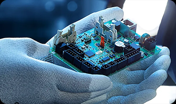
Fine-pitch components refer to integrated circuits (ICs) and other electronic parts with very close lead spacing, often 0.65mm (26 mil) or less. These components are essential for creating compact, high-performance devices like smartphones, wearables, and medical equipment. The smaller the pitch, the more components can fit into a limited space, enabling high-density PCB assembly.
However, the smaller size comes with a trade-off. The precision required for manufacturing and assembling these components is incredibly high. A slight misalignment or defect during the imaging process can lead to connection failures, short circuits, or reduced device performance. This is where fine pitch PCB imaging becomes a critical step in the production process.
Key Challenges in PCB Imaging for Fine-Pitch Components
Imaging is the process of transferring a circuit design onto a PCB substrate, typically through photolithography or other advanced techniques. For fine-pitch and micro-components, this process faces several obstacles. Let’s break down the most significant challenges in achieving PCB imaging accuracy.
1. Resolution Limitations
The first major challenge is achieving the necessary resolution to image fine-pitch patterns. As lead spacing shrinks to below 0.5mm in some cases, traditional imaging equipment may struggle to create clear, distinct lines and pads. If the resolution is too low, traces can blur or merge, leading to short circuits or open connections.
For example, a typical imaging system might have a resolution limit of 50 micrometers. However, for a micro-component PCB with 0.4mm pitch spacing, features as small as 20 micrometers may need to be resolved. Without advanced equipment, this level of detail is nearly impossible to achieve consistently.
2. Alignment and Registration Issues
In high-density PCB assembly, even a tiny misalignment during imaging can cause major problems. Registration refers to the alignment of different layers or features on a PCB. For fine-pitch components, a misalignment of just 10 micrometers can result in pads or vias being out of position, making it impossible to place or solder components accurately.
This issue is compounded in multi-layer boards, where each layer must align perfectly with the others. Poor registration can lead to signal integrity issues, especially in high-speed designs where impedance control is critical (e.g., maintaining 50 ohms for specific traces).
3. Material and Substrate Constraints
The choice of substrate material also impacts fine pitch PCB imaging. Some materials may shrink or expand during processing due to heat or humidity, distorting the imaged pattern. For instance, standard FR-4 material might have a dimensional stability of ±0.05%, which is acceptable for larger components but problematic for micro-pitch designs requiring tolerances of ±0.01% or better.
Additionally, the surface roughness of the substrate can interfere with imaging precision. A rough surface may scatter light during photolithography, reducing the clarity of fine traces and pads.
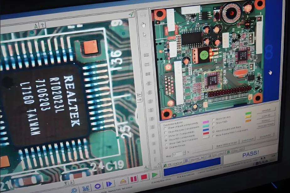
4. Defect Detection and Inspection
Detecting defects in fine-pitch imaging is another hurdle. With features so small, traditional visual inspection methods are often inadequate. Micro-cracks, incomplete traces, or over-etched areas might go unnoticed without specialized tools. These defects can lead to failures during assembly or in the field, especially for critical applications like automotive or aerospace electronics.
For example, a hairline crack in a 0.1mm trace might not be visible to the naked eye but could cause a 30% increase in resistance, disrupting signal flow at high frequencies (e.g., above 1 GHz).
Solutions to Overcome PCB Imaging Challenges
While the challenges of imaging fine-pitch components are significant, there are proven strategies and technologies to address them. Below, we outline actionable solutions for engineers and manufacturers working on small component PCB manufacturing.
1. Adopt Advanced Imaging Technologies
To tackle resolution limitations, manufacturers can invest in high-precision imaging systems like laser direct imaging (LDI). Unlike traditional photolithography, LDI uses a focused laser to directly write patterns onto the PCB, achieving resolutions down to 10 micrometers or better. This is ideal for micro-component PCB designs with ultra-fine features.
Additionally, digital imaging systems can reduce errors caused by film-based processes, as they eliminate the need for physical masks that can degrade over time. These systems also offer faster turnaround times, which is crucial for prototyping and small-batch production.
2. Improve Alignment with Automated Systems
Automated optical alignment systems can significantly enhance registration accuracy. These systems use high-resolution cameras and software to detect fiducial marks on the PCB, ensuring precise layer-to-layer alignment. Some advanced systems can achieve alignment tolerances of ±5 micrometers, well within the requirements for fine-pitch components.
Moreover, incorporating real-time feedback during the imaging process can help correct misalignments before they become permanent, reducing scrap rates in high-density PCB assembly.
3. Use High-Stability Materials
Selecting the right substrate material is key to minimizing distortion during imaging. High-performance materials like polyimide or advanced laminates offer better dimensional stability, with tolerances as low as ±0.01%. These materials are less prone to warping under heat or humidity, ensuring that fine-pitch patterns remain accurate throughout the manufacturing process.
For applications requiring extreme precision, manufacturers can also use thinner substrates (e.g., 0.2mm thick) to reduce stress and improve imaging consistency, though this may require adjustments in handling and processing.
4. Implement Advanced Inspection Techniques
To catch defects early, manufacturers should adopt automated optical inspection (AOI) and X-ray imaging for fine-pitch PCBs. AOI systems use high-resolution cameras to scan for surface defects like incomplete traces or misaligned pads, often detecting issues down to 10 micrometers in size.
For internal layers or hidden defects, X-ray inspection can reveal problems like voids or cracks that are invisible to standard cameras. These tools are essential for ensuring reliability in critical applications where a single defect could lead to catastrophic failure.
Best Practices for Fine-Pitch PCB Imaging
Beyond specific technologies, adopting certain best practices can further improve outcomes in fine pitch PCB imaging. These tips are designed to help manufacturers optimize their processes for better accuracy and yield.
- Design for Manufacturability (DFM): During the design phase, ensure that trace widths and spacings are within the capabilities of your imaging equipment. For instance, avoid designing 0.1mm traces if your system can only reliably image 0.15mm features.
- Control Environmental Factors: Maintain strict control over temperature and humidity in the imaging area to prevent material distortion. A stable environment (e.g., 22°C and 50% humidity) can reduce variability in results.
- Regular Calibration: Calibrate imaging and inspection equipment frequently to maintain precision. Even a small drift in calibration can lead to errors in fine-pitch designs.
- Collaborate with Experts: Work closely with imaging specialists to identify potential issues early. Their expertise can help tailor processes to the specific needs of your micro-component PCB project.
The Future of PCB Imaging for Fine-Pitch Components
As electronics continue to shrink, the demand for even finer pitch components will only grow. Emerging technologies like 3D imaging and artificial intelligence (AI) are poised to revolutionize small component PCB manufacturing. AI algorithms, for example, can predict and correct imaging errors in real-time, while 3D imaging can provide a more detailed view of multi-layer boards.
Additionally, advancements in materials science may lead to substrates with near-zero dimensional change, further improving PCB imaging accuracy. These innovations will be critical for next-generation applications, such as 5G devices requiring signal speeds above 10 Gbps or IoT sensors with ultra-compact footprints.
Conclusion
Imaging fine-pitch components on PCBs is no easy task. From resolution limits to alignment challenges, manufacturers face numerous obstacles in achieving the precision needed for high-density PCB assembly. However, with the right tools, materials, and practices, these challenges can be overcome. By adopting advanced imaging technologies, improving alignment systems, and implementing rigorous inspection methods, engineers can ensure reliable results for even the smallest components.
At the heart of successful fine pitch PCB imaging is a commitment to precision and innovation. As technology advances, staying ahead of the curve will be key to meeting the demands of modern electronics. Whether you’re working on a micro-component PCB or a complex multi-layer design, understanding and addressing imaging challenges is the first step toward building reliable, high-performance devices.


