 ALLPCB


When it comes to multi-layer PCB manufacturing, understanding the factors that drive costs is crucial for engineers and businesses aiming to optimize their budgets without sacrificing quality. The price of a multi-layer PCB is influenced by several key elements, including PCB layer count, material costs, via types, fabrication tolerances, and PCB size. In this detailed guide, we’ll break down each of these cost drivers to help you make informed decisions for your next project.
Whether you’re designing a complex circuit for a high-performance device or planning a bulk order for production, knowing what impacts the price can save you time and money. Let’s dive into the specifics of each factor, explore how they contribute to the overall cost, and provide actionable insights to manage expenses effectively.
Why Understanding PCB Manufacturing Costs Matters
Multi-layer PCBs are essential for modern electronics, offering compact designs and enhanced functionality for devices like smartphones, medical equipment, and industrial systems. However, their complexity often leads to higher production costs compared to single or double-layer boards. By understanding the cost drivers, you can balance performance needs with budget constraints, ensuring your project stays on track.
In the sections below, we’ll explore the primary factors affecting multi-layer PCB costs, supported by practical examples and data to give you a clear picture of what to expect.
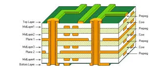
1. PCB Layer Count and Cost: More Layers, Higher Price
One of the most significant factors in multi-layer PCB pricing is the number of layers in the design. A multi-layer PCB can range from 4 to over 20 layers, with each additional layer increasing the manufacturing complexity and cost. Why does this happen?
Each layer requires additional materials, precise alignment during lamination, and more time for drilling and plating processes. For instance, a 4-layer PCB might be relatively affordable for basic applications, while a 12-layer board for high-density interconnect (HDI) designs could cost significantly more due to the intricate stacking and routing needed.
As a rough estimate, adding layers can increase costs by 30-40% per layer pair in smaller production runs. For high-volume orders, this percentage might decrease slightly due to economies of scale, but the base cost still rises with layer count. If you’re working on a project, consider whether all layers are necessary or if a simpler design could meet your requirements.
Tip: Optimize your layer count by planning signal routing early in the design phase. Reducing layers from 8 to 6, for example, could cut costs without impacting performance if done thoughtfully.
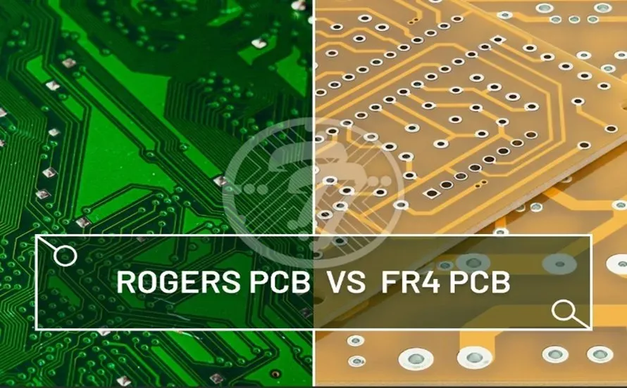
2. Material Costs for Multi-Layer PCBs: Quality Comes at a Price
The materials used in multi-layer PCBs play a major role in determining the final price. Standard materials like FR-4, a common fiberglass epoxy laminate, are widely used for their affordability and reliability in many applications. However, for high-frequency or high-temperature environments, specialized materials such as Rogers, Teflon, or polyimide are often required, and these come with a higher price tag.
For example, FR-4 might cost around $0.10 to $0.20 per square inch for a standard multi-layer board, while high-frequency materials could range from $0.50 to over $1.00 per square inch, depending on the grade and thickness. Additionally, the copper thickness (measured in ounces per square foot) affects cost—thicker copper (e.g., 2 oz instead of 1 oz) increases material expenses by 20-30% due to its higher conductivity needs.
Dielectric thickness between layers also matters. Thinner dielectrics, often needed for HDI designs, require more precision and specialized prepregs, further driving up costs. If your project doesn’t demand high-speed signals or extreme thermal resistance, sticking to standard materials can keep expenses in check.
3. Via Costs: Small Features with Big Price Impacts
Vias are the tiny holes that connect different layers in a multi-layer PCB, and their type, size, and quantity directly influence manufacturing costs. There are several types of vias, each with unique cost implications:
- Through-Hole Vias: These are the most common and cost-effective, as they pass through all layers of the board. They’re easier to drill and plate, keeping costs low.
- Blind Vias: These connect an outer layer to an inner layer without passing through the entire board. They require more precise drilling and additional processing steps, increasing costs by 20-50% compared to through-hole vias.
- Buried Vias: Hidden between inner layers, buried vias are even more expensive due to the need for sequential lamination and specialized equipment. Costs can be 50-100% higher than standard vias.
- Microvias: Used in HDI designs, microvias are extremely small (often less than 0.006 inches in diameter) and require laser drilling. They can add $0.05 to $0.15 per via to the manufacturing cost, depending on quantity and complexity.
The sheer number of vias also matters. A design with thousands of vias will naturally cost more than one with a few hundred due to the time and precision required. To manage via costs, minimize the use of blind, buried, or microvias unless they’re critical to your design’s performance.
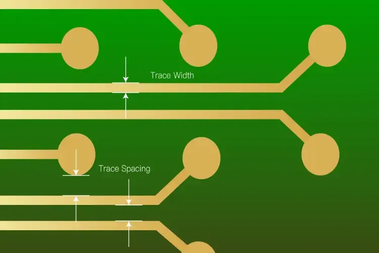
4. Fabrication Tolerances and Their Effect on Cost: Precision Isn’t Cheap
Fabrication tolerances refer to the precision required in manufacturing processes like drilling, etching, and layer alignment. Tighter tolerances mean higher costs because they demand advanced equipment, slower production speeds, and stricter quality control measures.
For example, a standard tolerance for trace width and spacing might be ±0.005 inches, which is achievable with conventional manufacturing techniques. However, if your design requires HDI features with tolerances of ±0.002 inches or less, the cost could increase by 25-50% due to the need for specialized machinery and additional inspection steps.
Similarly, drilling tolerances for via placement affect pricing. A standard drill tolerance of ±0.003 inches is cost-effective, but tighter tolerances for high-density designs can raise expenses. Layer-to-layer registration, critical for multi-layer boards, also becomes more expensive with tighter specs—misalignment as small as 0.001 inches can lead to signal integrity issues, so precision is non-negotiable in complex designs.
Tip: Work with your design team to relax tolerances where possible without compromising functionality. Even a small adjustment can lead to significant savings.
5. PCB Size and Cost: Bigger Boards, Bigger Bills
The physical size of your PCB directly impacts manufacturing costs. Larger boards require more raw materials, take up more space on production panels, and often need longer processing times. PCB size and cost are closely linked because manufacturers typically price boards based on square inches or square centimeters.
For instance, a small 2x2 inch board might cost a few dollars per unit in a multi-layer design, while a 10x10 inch board could cost 20-30 times more due to the increased material and processing requirements. Additionally, larger boards may reduce the number of units that fit on a standard production panel (often 18x24 inches), leading to higher per-unit costs.
Panel utilization is a key factor here. If your board size results in wasted space on the panel, you’re essentially paying for unused material. To optimize costs, consider designing your PCB to fit efficiently within standard panel sizes or explore panelization techniques to maximize yield.
Tip: If your design allows, split larger boards into smaller modules that can be assembled later. This can reduce material waste and lower costs significantly.
Other Factors Influencing Multi-Layer PCB Costs
Beyond the primary cost drivers, several other elements can affect the price of multi-layer PCBs:
- Production Volume: Small prototype runs are more expensive per unit due to setup fees and lack of economies of scale. Larger orders often reduce the cost per board by spreading fixed expenses across more units.
- Surface Finish: Options like ENIG (Electroless Nickel Immersion Gold) or HASL (Hot Air Solder Leveling) vary in price. ENIG, for instance, can add $0.05 to $0.10 per square inch compared to HASL due to its superior corrosion resistance and flatness.
- Testing Requirements: Rigorous testing, such as electrical testing or impedance control (e.g., maintaining 50 ohms for high-speed signals), adds to the cost. Impedance testing might increase expenses by 10-20% depending on the complexity.
By factoring in these additional considerations during the planning stage, you can avoid unexpected expenses and keep your project within budget.
How to Optimize Multi-Layer PCB Costs Without Sacrificing Quality
Balancing cost and quality is a challenge, but it’s achievable with strategic planning. Here are some practical ways to reduce expenses:
- Simplify Your Design: Minimize layer count and avoid over-specifying tolerances or materials unless necessary for performance.
- Choose Cost-Effective Materials: Use standard materials like FR-4 for non-critical applications and reserve high-end options for specific needs.
- Plan for Efficient Panelization: Design your PCB size to maximize the number of boards per production panel, reducing waste.
- Limit Complex Features: Reduce the use of blind or buried vias and microvias unless they’re essential for your design.
- Partner with Experts: Collaborate with a reliable manufacturing team to get design-for-manufacturability (DFM) feedback early in the process.
Implementing these strategies can help you achieve a high-quality multi-layer PCB while keeping costs under control.
Conclusion: Take Control of Your Multi-Layer PCB Costs
Understanding the cost drivers behind multi-layer PCB manufacturing empowers you to make smarter decisions for your projects. From PCB layer count and material costs to via types, fabrication tolerances, and board size, each element plays a role in determining the final price. By carefully evaluating your design needs and optimizing where possible, you can achieve the performance you require without breaking the bank.
At ALLPCB, we’re committed to helping you navigate these complexities with transparent pricing and expert support. Whether you’re working on a prototype or a large-scale production run, our team is ready to assist in bringing your multi-layer PCB designs to life at a competitive cost. Start planning your next project with these insights in mind, and you’ll be well on your way to success.


