 ALLPCB


In the fast-paced world of electronics, miniaturization is key to creating smaller, more powerful devices. Embedded Component Technology in PCBs (Printed Circuit Boards) is revolutionizing how we design and manufacture electronics by integrating components directly into the board’s layers. This approach saves space, boosts performance, and enhances reliability. But what equipment is essential for embedding components in PCBs? At the core, you need tools for cavity formation, thin-film deposition, high-precision placement, and testing embedded component PCBs. In this detailed guide, we’ll explore the cutting-edge equipment driving this technology and how it’s shaping a new era of miniaturization.
What Is Embedded Component Technology in PCBs?
Embedded Component Technology involves placing electronic components, such as resistors, capacitors, or even active devices like ICs, directly into the internal layers of a PCB. Unlike traditional surface-mount technology (SMT), where components sit on the board’s surface, embedding reduces the overall footprint, improves signal integrity, and enhances durability by protecting components from external damage. This technique is a game-changer for industries like automotive, medical, and consumer electronics, where space and reliability are critical.
The process requires specialized equipment to create cavities, deposit materials, place components with pinpoint accuracy, and test the final product. Let’s dive into the specific tools and technologies that make embedding components in PCBs possible.
Equipment for Cavity Formation in PCBs
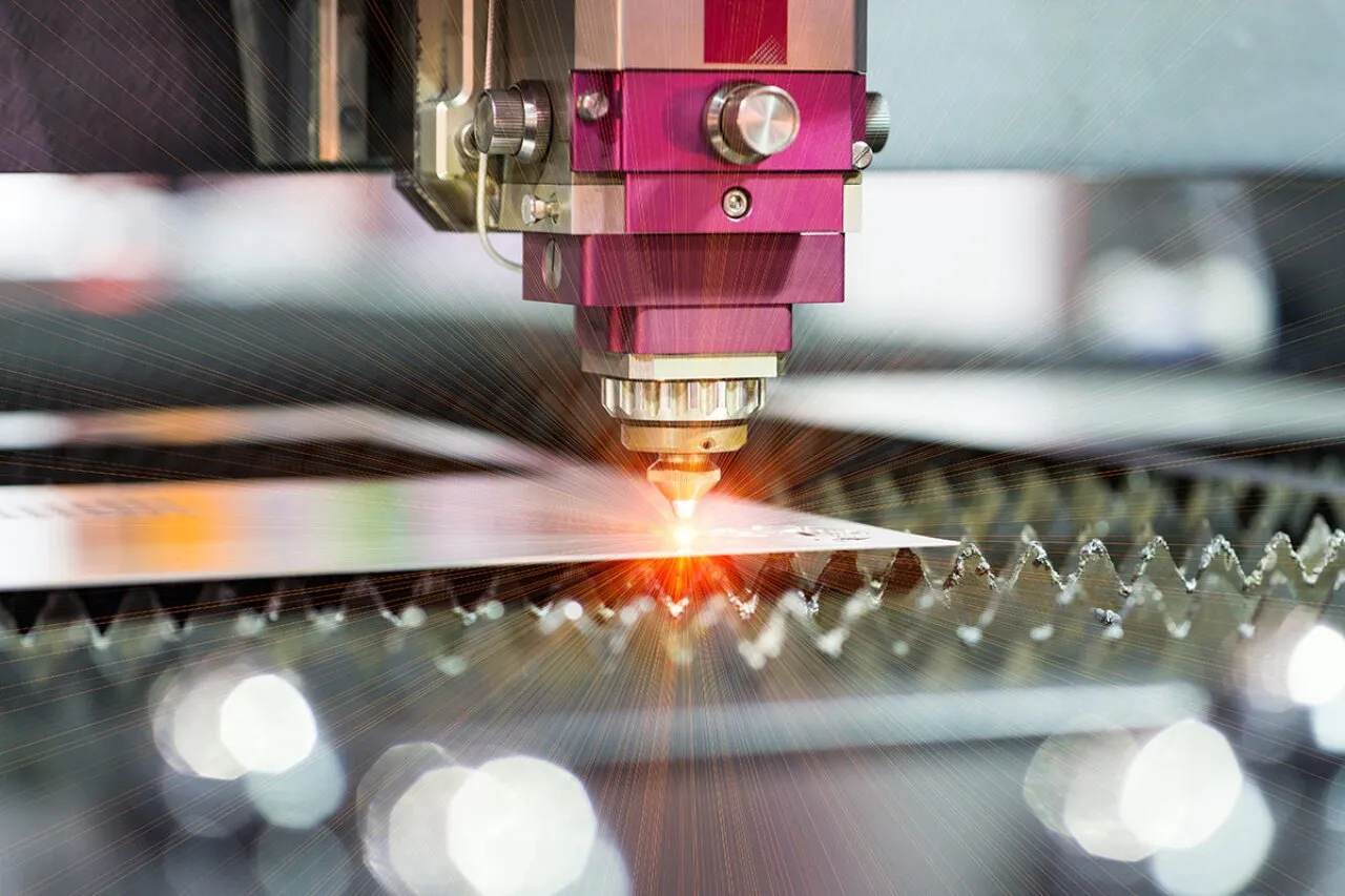
Cavity formation is the first critical step in embedding components. A cavity is a small recess or pocket created within the PCB layers to house the component. Precision is vital to ensure the component fits perfectly and maintains electrical connections. Here are the primary tools used for cavity formation:
- Laser Drilling Systems: Laser drilling machines use focused beams to cut precise cavities into the PCB substrate or prepreg material. These systems can achieve accuracies down to 10 micrometers, ensuring the cavity matches the component’s dimensions. Advanced lasers, such as UV or CO2 lasers, are often used for their ability to handle various materials without causing thermal damage.
- CNC Milling Machines: For larger cavities or thicker boards, Computer Numerical Control (CNC) milling machines provide a mechanical alternative to lasers. These machines use high-speed rotating tools to carve out cavities with tolerances as tight as 50 micrometers. They are ideal for prototyping or low-volume production.
- Plasma Etching Equipment: Plasma etching uses ionized gas to remove material selectively, creating cavities with smooth edges. This method is particularly useful for complex multilayer boards where precision and surface quality are paramount.
Using the right equipment for cavity formation in PCBs ensures that components are securely embedded without compromising the board’s structural integrity. Poorly formed cavities can lead to misalignment, electrical failures, or mechanical stress, so investing in high-quality tools is essential.
Thin-Film Deposition for Embedded Components
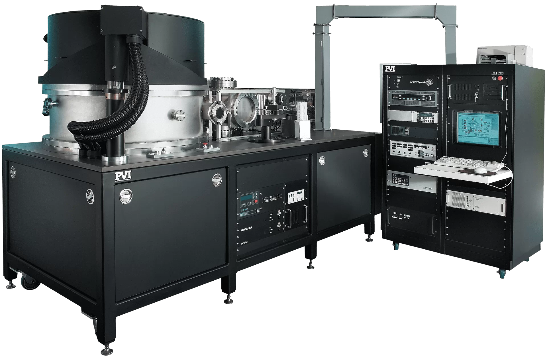
Once cavities are formed, thin-film deposition plays a crucial role in creating conductive paths and protective layers around embedded components. This process involves applying ultra-thin layers of materials, often metals or insulators, to ensure reliable electrical connections and insulation. The following equipment is commonly used for thin-film deposition for embedded components:
- Sputtering Systems: Sputtering involves bombarding a target material with high-energy particles to deposit a thin film onto the PCB. This method is ideal for creating conductive layers, such as copper or gold, with thicknesses as low as 100 nanometers. It ensures uniform coverage even in complex cavity structures.
- Chemical Vapor Deposition (CVD) Machines: CVD uses chemical reactions to deposit thin films from a gas phase. This technique is often used for insulating layers, like silicon dioxide, which protect embedded components from electrical interference. CVD offers excellent control over film thickness, often achieving uniformity within 5% variation.
- Atomic Layer Deposition (ALD) Tools: ALD is a highly precise method that deposits materials one atomic layer at a time. It’s perfect for ultra-thin insulating or barrier layers, ensuring minimal defects in high-density PCB designs. ALD equipment can achieve layer thicknesses as small as 0.1 nanometers.
Thin-film deposition for embedded components is critical for maintaining signal integrity and protecting delicate parts. For example, a poorly deposited conductive layer could increase impedance, leading to signal delays or losses. Modern deposition tools help engineers achieve the precision needed for cutting-edge miniaturized designs.
High-Precision Placement of Embedded Components
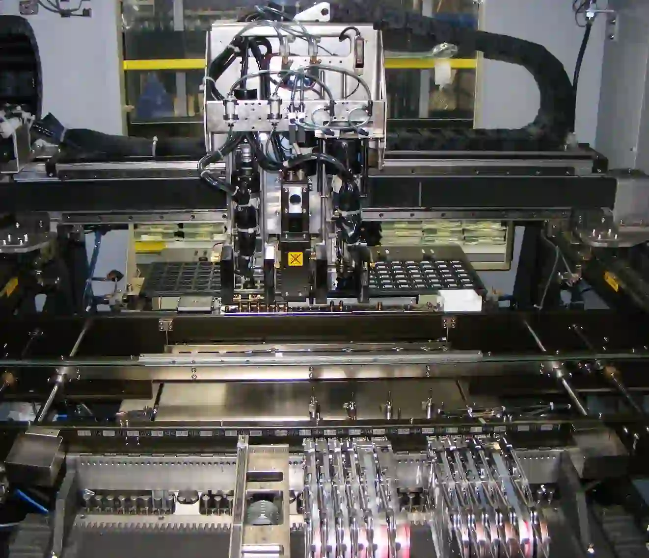
Placing components into PCB cavities with high accuracy is a challenging but essential step. Even a slight misalignment can disrupt electrical connections or cause mechanical stress. The equipment for high-precision placement of embedded components includes advanced tools designed for accuracy and speed:
- Pick-and-Place Machines: Modern pick-and-place systems are equipped with vision systems and robotic arms to position components with accuracies of up to 10 micrometers. These machines can handle a wide range of components, from tiny resistors to complex ICs, placing them directly into cavities or onto designated layers before lamination.
- Die Bonding Equipment: For bare die embedding, die bonding tools use heat and pressure to attach semiconductor chips directly into the PCB. These systems often include alignment cameras and automated controls to ensure placement errors are below 5 micrometers, critical for high-performance applications.
- 3D Assembly Platforms: Some advanced platforms integrate 3D imaging and robotic systems to place components in multilayer cavities. These tools are particularly useful for complex designs where components are stacked or embedded at different depths within the PCB.
High-precision placement of embedded components ensures that the final product meets strict performance standards. For instance, in high-frequency applications, a misplaced component could alter signal paths, increasing impedance by as much as 20% and degrading performance. The right equipment minimizes such risks, paving the way for reliable miniaturization.
Testing Embedded Component PCBs
After embedding components, thorough testing is necessary to ensure functionality and reliability. Since embedded components are not easily accessible for rework, testing embedded component PCBs requires specialized equipment to detect faults without damaging the board. Here are the key tools used:
- X-Ray Inspection Systems: X-ray machines provide non-destructive testing by creating detailed images of internal PCB layers. They can detect misalignments, voids in solder joints, or cracks in embedded components with resolutions down to 1 micrometer. This is crucial for quality control in high-density designs.
- Automated Optical Inspection (AOI) Equipment: AOI systems use high-resolution cameras and software to inspect the PCB surface and near-surface layers. While they can’t see deep into the board, they complement X-ray systems by checking for surface defects or alignment issues post-lamination.
- In-Circuit Testers (ICT): ICT equipment uses probes to test electrical connections and component functionality within the PCB. Modern testers can measure impedance, resistance, and capacitance with accuracies of 1%, ensuring that embedded components perform as expected. For example, a capacitor with an impedance deviation of more than 5% could indicate a placement or connection issue.
- Thermal Imaging Cameras: These cameras detect heat signatures during operation to identify overheating components or poor connections. They are especially useful for power-intensive embedded designs where thermal management is critical.
Testing embedded component PCBs is the final safeguard against failures in the field. A single undetected fault, such as a misaligned connection increasing signal delay by 10 nanoseconds, could render a device unusable. Advanced testing equipment ensures that miniaturized designs meet the highest standards of quality and performance.
Benefits of Embedded Component Technology for Miniaturization
The use of specialized equipment for embedding components in PCBs unlocks several advantages that drive miniaturization:
- Space Savings: Embedding components can reduce the PCB footprint by up to 40%, allowing for smaller devices without sacrificing functionality. This is vital for wearables, IoT devices, and medical implants.
- Improved Signal Integrity: By shortening connection lengths, embedded designs can reduce signal loss and interference. For high-speed applications, this can improve signal speeds by 15-20% compared to surface-mounted setups.
- Enhanced Reliability: Components embedded within the PCB are protected from environmental factors like moisture and vibration, increasing the lifespan of the device by as much as 30% in harsh conditions.
- Cost Efficiency: While initial equipment costs are high, embedding can lower assembly costs by reducing the number of soldering steps and minimizing external components, saving up to 10-15% in high-volume production.
These benefits highlight why industries are rapidly adopting embedded component technology as a cornerstone of modern electronics design.
Challenges and Future Trends in Embedded Component Technology
Despite its advantages, embedding components in PCBs comes with challenges. The high cost of equipment, such as laser drilling systems or ALD tools, can be a barrier for smaller manufacturers. Additionally, the complexity of testing embedded designs requires ongoing investment in advanced inspection tools. Thermal management is another concern, as densely packed components can generate heat, potentially raising temperatures by 10-15°C above safe limits if not addressed.
Looking ahead, the future of embedded component technology is promising. Innovations like 3D-integrated circuits and advanced packaging techniques are pushing the boundaries of miniaturization. Equipment manufacturers are also developing more affordable and automated tools, making the technology accessible to a broader range of businesses. For instance, hybrid laser-CNC systems are emerging to combine precision and cost-effectiveness for cavity formation.
Conclusion: Embracing the New Era of Miniaturization
Embedded Component Technology in PCBs is transforming the electronics industry by enabling unprecedented levels of miniaturization. From laser drilling systems for cavity formation to sputtering tools for thin-film deposition, high-precision placement machines, and advanced testing equipment, the tools behind this technology are driving innovation. By understanding and leveraging the right equipment for embedding components in PCBs, manufacturers can create smaller, faster, and more reliable devices that meet the demands of today’s market.
As this technology continues to evolve, staying updated on the latest equipment and techniques will be crucial for engineers and designers. The era of miniaturization is here, and with the right tools, the possibilities for creating compact, high-performance electronics are endless. Whether you’re working on a cutting-edge IoT device or a life-saving medical tool, embedded component technology offers the solutions you need to push boundaries and achieve excellence.


