Introduction
In the world of PCB manufacturing, precision, cost-effectiveness, and efficiency are essential. One often overlooked yet crucial feature in panelized PCB fabrication is the use of mouse bites PCB designs. Mousebites are tiny perforated holes along the edges of a PCB that allow individual boards to be easily broken off from a larger panel after assembly.
Mouse bites PCB technology is particularly useful in scenarios like surface mount technology (SMT) assembly, hand-assembled prototypes, and low-volume production runs. Their implementation can streamline the depanelization process, reduce tooling costs, and offer greater flexibility for irregular board shapes.
In this complete guide, we will explore what mouse bites PCB are, how they compare to other separation methods, and when and why to use them in your next PCB project.
What is Mouse Bites PCB (Mousebites) in Manufacturing?
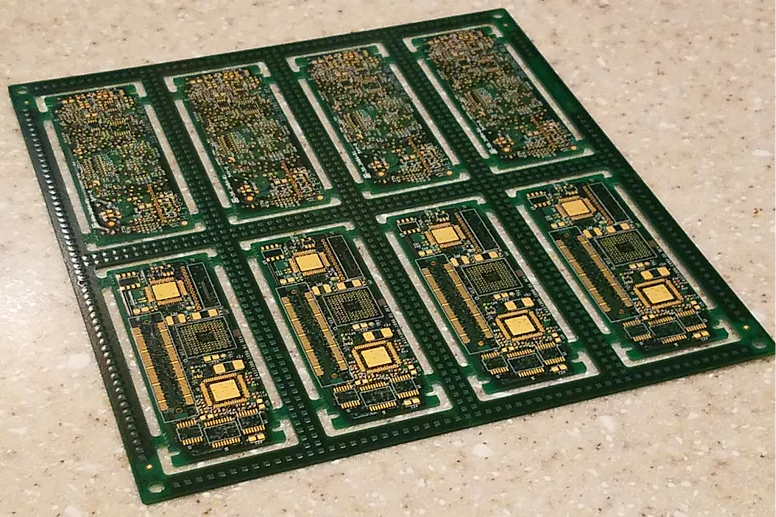
The mouse bites, also called perforated breakaway tabs or pcb breakaway tabs, are the sharp edges left over after stamp hole depanelization when PCBs are manufactured in a panel using break-routing/break-off tabs. Mouse bite PCB structures consist of a line of tiny holes in a circuit board—just like the holes around postage stamps—permitting small PCBs to be used in an array.
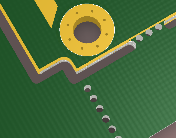
These rows of holes earned the nickname "mouse bites" because the indentations left behind after they break resemble the bite marks of a mouse that nibbled on the board. Mousebite PCB perforation is standard for FR4 panels. Drilling these holes leaves rough edges of extra material sticking out the side, while a V-groove PCB with a V-scored edge is smoother.
In PCB manufacturing, especially for PCB designs, mousebites are a common technique used when multiple small boards are grouped into a larger panel for easier assembly and processing. This method allows for easy separation after the assembly stage, which is crucial for efficiency, especially in high-mix low-volume production.
Why Use Mouse Bites PCB and Breakaway Tabs?
Mouse bites PCB serve several purposes in custom fabrication:
- Ease of Separation: They allow individual boards to be snapped out of a larger panel without complex tools.
- Better Grip: When a board must be mounted or inserted into a tight slot, mousebite PCB edges help create a textured grip.
- Cost-Effective for Hand Separation: Particularly for small runs or prototypes, this method reduces labor and tool requirements.
- Design Flexibility: They're ideal for oddly shaped boards, where pcb breakaway tabs are more suitable than V-scoring.
While standard on FR4 PCBs, mouse bites are also compatible with other substrates like aluminum PCB boards, though special care must be taken during the depanelization of metal-core materials due to their added thickness and rigidity.
Mousebite PCB Design: How to Place Breakaway Tabs
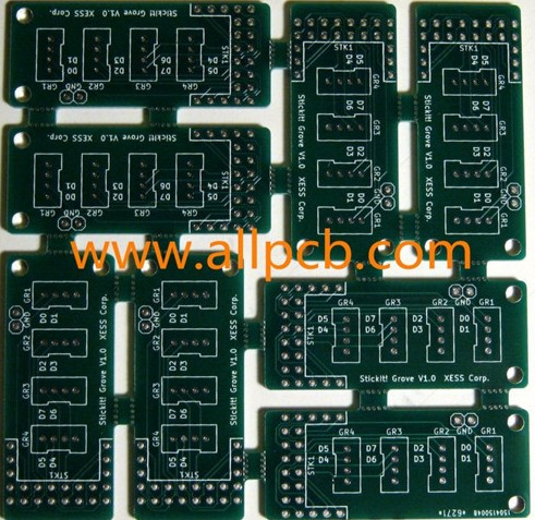
If you panelize individual PCBs within the panel, you only need to mouse bite the PCB edge. For routed boards, mousebites are typically seen on both the rail side and the board side. Routing a board and adding mouse bite PCB tabs is more expensive than a simple v-score, but non-rectangular outlines rely on this method.
One important aspect is to have a clean edge after the breakaway tab is removed. Slight inset perforations are preferred because they leave an edge requiring little to no post-processing.
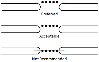
The spacing between PCB breakaway tabs can range from 60 mm to 90 mm, but I recommend 77 mm from center to center as shown in Figure 3. Try not to exceed 100 mm between tabs and try to evenly space them apart.

How Mouse Bites PCB Panelization Works
Mouse bites are used during the panelization process to create an array of PCBs that can be processed together during assembly. Here’s how it works:
- Multiple PCBs are arranged into a single panel, connected by PCB breakaway tabs.
- These tabs contain lines of drilled mousebite holes.
- After assembly and soldering, the individual boards can be snapped out by hand or using tools like pliers.
The drilled holes weaken the connection enough to allow for easy separation, yet maintain panel strength during the manufacturing process.
Slight inset of perforation is preferred because it provides an edge which requires little to no additional labor to clean up.
Learn more in our detailed guide: Mouse Bites Panelization for SMT Assembly
Mousebites PCB vs. V-Scoring: Which to Choose?
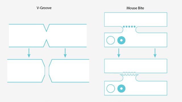
It’s worth noting the difference between mouse bites PCB and V-scored PCBs.
- V-scoring: Cuts V-shaped grooves into the panel, resulting in smooth edges.
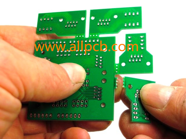
- Mousebites: Use a line of perforated holes, leaving jagged edges unless sanded.
While not as clean as V cut PCB edges, mouse bites are more suitable for curved edges or irregular board outlines. That said, for applications where smooth edges are not critical, mouse bites provide a faster and more flexible depanelization option. They are particularly advantageous when laser direct imaging is used for creating highly detailed and compact circuit designs, where board shapes might be irregular or compact spacing is needed.
Suggested Reading: V-Scoring vs. Stamp Hole Depaneling: Choosing the Right Method for Your PCB
Cost-Saving Benefits of Mouse Bites PCB
One of the primary reasons manufacturers prefer mousebites PCB is their cost-effectiveness. Here are the ways mouse bites can help reduce overall manufacturing expenses:
- No special cutting equipment required: Unlike V-scoring or routing, mouse bites can be created using standard CNC drilling machines.
- Lower labor costs: Boards can be manually snapped apart without advanced machinery.
- Reduced panel waste: Enables more flexible PCB breakaway tabs design, optimizing panel utilization.
- Ideal for low-volume runs: Great for prototyping and small-batch productions where tooling costs must be minimized.
See how mouse bites impact your bottom line: Cost-Effective PCB Manufacturing: How Mouse Bites Can Save You Money
When to Use Mousebites PCB in Prototyping and Hand Assembly
For low-volume, hand-assembled PCBs—such as in prototyping, research labs, or startups—mousebites PCB offer a reliable and low-cost solution.
- No need for depaneling equipment
- Easy to break by hand with pliers
- Can be combined with fiducials for alignment
This method is especially useful in early development stages where speed, cost, and accessibility are key.
Discover real-world applications: Mouse Bites are a life saver in hand assembled PCBs
Strength and Reliability of Mouse Bite PCB Edges
A concern with mouse bite PCB depanelization is structural strength after snapping. Breaking tabs may leave:
- Rough edges (which may need sanding)
- Potential microcracks if not handled properly
- Slightly weaker corner strength compared to routed or scored boards
However, with proper design considerations—such as increasing the tab width, using fewer mouse bites per tab, and post-break sanding—these issues can be mitigated.
Learn about durability: The Impact of Mouse Bites on PCB Strength and Reliability
ALLPCB: Your Partner in Precision Mouse Bites PCB Manufacturing
Mouse bites offer a practical and economical approach to PCB panelization and depaneling. Whether you're creating early-stage prototypes, managing hand-assembled boards, or optimizing for cost-efficiency, this method provides a flexible solution that balances quality and ease of use.
At ALLPCB, we specialize in high-precision, custom PCB fabrication—including expertly designed mousebite PCB layouts for seamless panelization and clean depaneling. Whether you need rigid-flex PCBs, durable aluminum PCB boards, or advanced HDI solutions using laser direct imaging (LDI), our team ensures your boards are manufactured with unmatched accuracy and consistency.
From quick-turn prototypes to complex multi-layer arrays with PCB breakaway tabs, ALLPCB helps you reduce lead times, control custom PCB cost, and maintain the highest manufacturing standards. Let us be your trusted partner in building smarter, cleaner, and more efficient PCBs—designed with mousebites that work.
 ALLPCB


