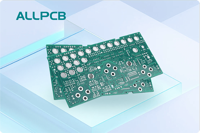
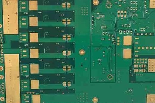
In the fast-evolving world of electronics, High-Density Interconnect (HDI) PCB manufacturing is pushing boundaries to meet the demands of smaller, faster, and more powerful devices. One technology at the forefront of this transformation is PCB direct imaging, a game-changer that moves beyond traditional phototools. But what exactly is PCB direct imaging, and how does it revolutionize HDI manufacturing? Simply put, PCB direct imaging, often referred to as laser direct imaging (LDI), uses lasers to directly transfer circuit patterns onto a board, eliminating the need for physical masks or phototools. This results in finer lines, higher precision, and faster production for HDI PCBs.
In this blog, we’ll dive deep into how HDI PCB direct imaging transforms fine line PCB manufacturing, the benefits of laser direct imaging for HDI, and why maskless lithography is becoming a cornerstone for high-density interconnect PCB production. Whether you’re an engineer designing compact electronics or a manufacturer looking to optimize processes, this guide will walk you through the essentials of this cutting-edge technology.
What Is PCB Direct Imaging and Why Does It Matter for HDI?
PCB direct imaging is a modern fabrication technique that uses laser or digital imaging to create circuit patterns directly on a photoresist-coated PCB substrate. Unlike traditional methods that rely on phototools—physical masks or films used to expose patterns—direct imaging eliminates intermediary steps, offering unmatched accuracy and flexibility. For high-density interconnect PCB designs, where space is limited and precision is critical, this technology is a perfect fit.
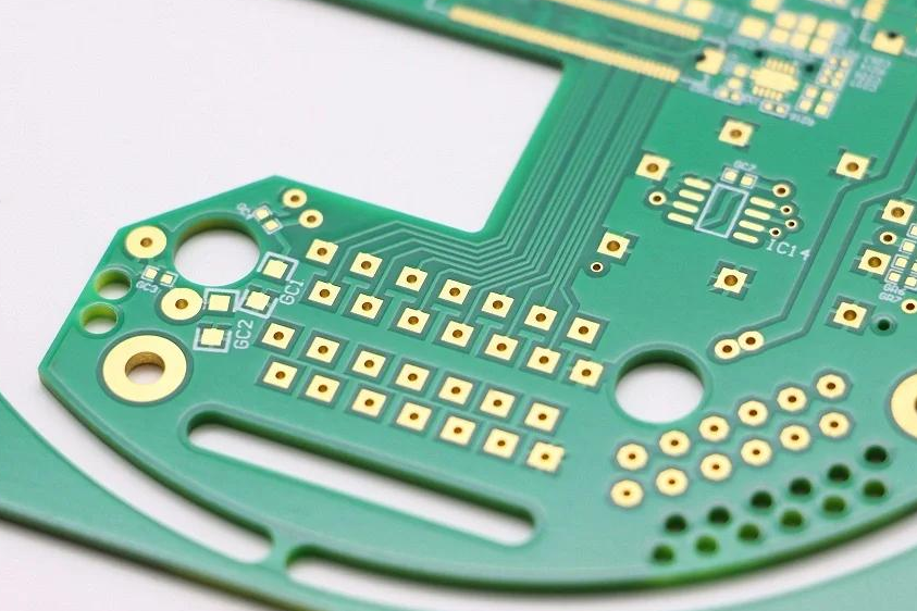
HDI PCBs are defined by their high circuitry density, often incorporating microvias (vias smaller than 0.15 mm in diameter), blind and buried vias, and fine line traces (widths as narrow as 25 microns). These features enable compact designs for smartphones, wearables, and automotive electronics. However, achieving such precision with traditional phototools can be challenging due to alignment errors and the physical limitations of masks. Laser direct imaging for HDI overcomes these hurdles by providing sub-micron resolution and precise control over line widths, ensuring that even the most intricate designs are manufactured flawlessly.
The Evolution from Phototools to Maskless Lithography in PCB Manufacturing
Historically, PCB manufacturing relied heavily on phototools, which are films or masks created from design data to expose photoresist layers on a board. While effective for simpler designs, this method struggles with the demands of fine line PCB manufacturing. Misalignment, wear and tear of masks, and the time-consuming process of creating and adjusting phototools often lead to delays and defects in HDI production.
Enter maskless lithography for PCBs, a core principle behind PCB direct imaging. This approach uses digital data to guide a laser or light source, directly patterning the photoresist without any physical intermediary. The result? Faster setup times, reduced costs from eliminating mask production, and the ability to make real-time adjustments to designs. For HDI PCB direct imaging, this means manufacturers can achieve trace widths and spacing as tight as 20-30 microns, a feat nearly impossible with traditional methods due to diffraction limits and alignment issues.
Moreover, maskless lithography supports rapid prototyping. Since there’s no need to fabricate a new mask for every design change, engineers can iterate quickly, testing multiple layouts in a fraction of the time. This agility is invaluable in industries like consumer electronics, where time-to-market is critical.
How Laser Direct Imaging Enhances Fine Line PCB Manufacturing
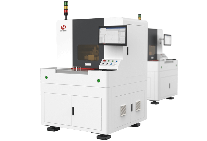
Laser direct imaging (LDI) is the most widely used form of PCB direct imaging, and its impact on fine line PCB manufacturing is profound. LDI systems use a focused laser beam to expose photoresist with extreme precision, achieving resolutions down to 10 microns or less. This level of detail is essential for HDI designs, where signal integrity depends on tightly controlled impedance values—often within ±10% of the target (e.g., 50 ohms for high-speed signals).
One key advantage of laser direct imaging for HDI is its ability to handle complex multilayer boards. HDI PCBs often feature 6 to 12 layers or more, with microvias connecting them in intricate patterns. LDI ensures that each layer’s traces and vias align perfectly, reducing signal loss and crosstalk, which can degrade performance at high frequencies (e.g., above 1 GHz). Additionally, LDI minimizes defects like over- or under-exposure, which are common with phototools due to inconsistent light distribution.
Another benefit is scalability. As devices shrink and demand for finer lines grows—think trace widths of 25 microns for 5G applications—LDI systems can adapt by adjusting laser focus and intensity. This flexibility makes it a future-proof solution for high-density interconnect PCB production.
Key Benefits of HDI PCB Direct Imaging for Manufacturers and Engineers
The shift to PCB direct imaging brings a host of advantages, especially for HDI manufacturing. Let’s break down the most impactful benefits:
- Higher Precision and Quality: With laser direct imaging for HDI, manufacturers can achieve line widths and spacing below 30 microns with near-perfect accuracy. This reduces defects and ensures consistent performance in high-speed applications.
- Faster Production Cycles: Eliminating phototools cuts down setup time significantly. A design change that might take days with traditional methods (due to mask fabrication) can be implemented in hours using maskless lithography for PCBs.
- Cost Efficiency: While the initial investment in LDI equipment is higher, the long-term savings are substantial. There’s no recurring cost for masks, and fewer errors mean less material waste.
- Enhanced Design Flexibility: Engineers can experiment with complex HDI layouts without worrying about the limitations of physical masks. Real-time adjustments during imaging allow for on-the-fly optimization.
- Environmental Benefits: Traditional phototool processes often involve chemicals and materials for mask production, contributing to waste. Direct imaging reduces this footprint, aligning with sustainable manufacturing practices.
These benefits make HDI PCB direct imaging not just a technological upgrade but a strategic choice for staying competitive in industries like telecommunications, medical devices, and automotive electronics.
Applications of Laser Direct Imaging in High-Density Interconnect PCB Production
The versatility of laser direct imaging for HDI extends to a wide range of applications, each with unique demands for precision and performance. Here are some key areas where this technology shines:
- Consumer Electronics: Smartphones, tablets, and wearables rely on HDI PCBs to pack powerful components into tiny spaces. LDI enables trace widths as small as 20 microns, supporting high-speed data transfer rates (up to 10 Gbps) for 5G and beyond.
- Automotive Systems: Advanced driver-assistance systems (ADAS) and electric vehicle control units require multilayer HDI boards with robust signal integrity. Direct imaging ensures precise via placement and minimal crosstalk, critical for safety and performance.
- Medical Devices: From pacemakers to imaging equipment, medical electronics demand compact, reliable PCBs. Maskless lithography for PCBs allows for intricate designs that meet stringent regulatory standards.
- Telecommunications: High-frequency applications like 5G base stations need HDI PCBs with tightly controlled impedance (e.g., 50 ohms ±5%). LDI delivers the precision needed for consistent signal quality.
In each of these sectors, the ability to produce fine line PCB manufacturing with speed and accuracy gives manufacturers a significant edge, enabling innovation and meeting market demands.
Challenges and Considerations in Adopting PCB Direct Imaging
While the advantages of HDI PCB direct imaging are clear, there are challenges to consider before adoption. First, the upfront cost of LDI equipment can be a barrier for smaller manufacturers. High-end systems often range from hundreds of thousands to millions of dollars, though the return on investment comes from reduced operational costs over time.
Second, the technology requires skilled operators and robust software integration. Design files must be optimized for direct imaging, and any errors in data preparation can lead to costly mistakes. Training staff and ensuring compatibility with existing workflows are essential steps.
Finally, while laser direct imaging excels at fine line PCB manufacturing, it may not be the best fit for very high-volume production of simpler designs. Traditional phototools can still be more cost-effective for basic, large-scale runs where precision isn’t as critical.
Despite these challenges, the long-term benefits of precision, speed, and flexibility make direct imaging a worthwhile investment for HDI-focused manufacturers.
The Future of Maskless Lithography in HDI PCB Manufacturing
As electronics continue to shrink and performance demands grow, the role of maskless lithography for PCBs will only expand. Emerging trends point to even finer resolutions—potentially below 10 microns—as laser technology advances. Additionally, integration with automation and AI-driven design tools could further streamline the imaging process, reducing human error and optimizing layouts for signal speeds exceeding 25 Gbps.
Another exciting development is the potential for hybrid imaging systems that combine laser direct imaging with other techniques for specialized applications. For instance, combining LDI with inkjet printing could enable rapid prototyping of flexible HDI PCBs for wearable tech.
For manufacturers, staying ahead means adopting technologies like HDI PCB direct imaging now, building the expertise and infrastructure to handle tomorrow’s challenges. The shift from phototools to digital, maskless solutions isn’t just a trend—it’s the future of high-density interconnect PCB production.
Conclusion: Embracing the Direct Imaging Revolution for HDI Success
PCB direct imaging, powered by laser direct imaging technology, is transforming HDI manufacturing by leaving behind the limitations of traditional phototools. With its ability to deliver unparalleled precision for fine line PCB manufacturing, accelerate production cycles, and support complex high-density interconnect PCB designs, this technology is a must-have for modern electronics fabrication.
From achieving trace widths of 20-30 microns to enabling rapid design iterations, HDI PCB direct imaging addresses the core needs of industries pushing the boundaries of innovation. While challenges like initial costs and training exist, the benefits of quality, efficiency, and sustainability far outweigh them. As we look to the future, maskless lithography for PCBs will continue to redefine what’s possible, paving the way for smaller, smarter, and more powerful devices.
At ALLPCB, we’re committed to leveraging cutting-edge solutions like laser direct imaging for HDI to help engineers and manufacturers bring their visions to life. Whether you’re designing the next generation of 5G devices or compact medical equipment, direct imaging is your key to success in the world of HDI manufacturing.
 ALLPCB


