ALLPCB


In the fast-paced world of electronics, designing printed circuit boards (PCBs) for high-frequency applications is a complex yet critical task. When it comes to sequential build-up PCBs, ensuring signal integrity and performance in high-frequency environments is paramount. So, what are the key considerations for designing sequential build-up PCBs for high-frequency applications? The answer lies in focusing on impedance control, material selection, layer stack-up, and manufacturing precision to maintain signal integrity and minimize losses.
In this comprehensive guide, we'll dive deep into the essentials of sequential build-up PCB design, particularly for high-frequency applications like RF (radio frequency) systems. Whether you're an engineer working on cutting-edge telecommunications equipment or developing advanced radar systems, understanding these design principles will help you achieve optimal performance. Let's explore the critical factors surrounding sequential build-up PCB signal integrity, high-frequency PCB sequential build-up, impedance control sequential build-up, and sequential build-up materials for RF PCBs.
What Are Sequential Build-Up PCBs and Why Are They Important?
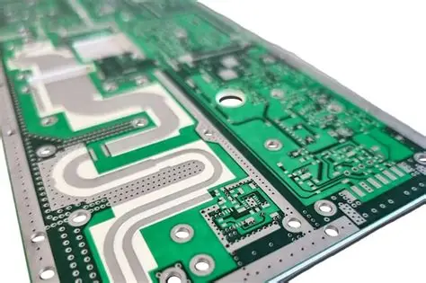
Sequential build-up (SBU) PCBs, also known as high-density interconnect (HDI) boards, are designed by adding layers step-by-step during the manufacturing process. Unlike traditional multilayer PCBs, where all layers are laminated at once, SBU technology allows for finer traces, smaller vias, and higher component density. This makes them ideal for compact, high-performance devices, especially in high-frequency applications where space and signal quality are critical.
In high-frequency systems, such as those operating above 1 GHz, signal integrity becomes a major concern. Even minor disruptions, like signal reflections or crosstalk, can degrade performance. Sequential build-up PCBs address these challenges by enabling precise control over layer thickness, trace geometry, and dielectric properties. This precision is essential for maintaining consistent signal paths and minimizing losses in RF and microwave applications.
Key Design Considerations for High-Frequency PCB Sequential Build-Up
Designing sequential build-up PCBs for high-frequency applications requires careful attention to several factors. Below, we break down the most important considerations to ensure your design meets performance expectations.
1. Impedance Control in Sequential Build-Up PCBs
Impedance control is a cornerstone of high-frequency PCB design. In sequential build-up boards, maintaining a consistent characteristic impedance (often 50 ohms for RF systems) across signal traces is vital to prevent signal reflections and ensure efficient power transfer. Even a small mismatch can lead to significant signal loss or distortion at frequencies above 1 GHz.
To achieve impedance control in sequential build-up designs, consider the following:
- Trace Width and Spacing: The width of a trace and its spacing from ground planes directly affect impedance. For a 50-ohm impedance, a microstrip trace on a standard FR-4 material might require a width of approximately 6 mils with a dielectric thickness of 4 mils. Use simulation tools to calculate exact dimensions based on your stack-up.
- Dielectric Thickness: Thinner dielectric layers in SBU designs allow for tighter control over impedance but require precise manufacturing to avoid variations.
- Via Design: Microvias and blind vias, common in SBU PCBs, must be optimized to minimize inductance and impedance discontinuities. Keep via stubs as short as possible, ideally less than 10 mils, to reduce parasitic effects.
2. Material Selection for RF PCBs with Sequential Build-Up
The choice of materials plays a huge role in the performance of high-frequency PCBs. When it comes to sequential build-up materials for RF PCBs, low dielectric constant (Dk) and low dissipation factor (Df) are critical to minimize signal loss and maintain integrity at high frequencies.
Here are some key points to guide material selection:
- Low-Loss Dielectrics: Materials like PTFE-based laminates or ceramic-filled composites often have a Dk of around 2.2 to 3.5 and a Df below 0.002, making them ideal for RF applications operating at 5 GHz or higher.
- Thermal Stability: High-frequency designs often generate heat, so materials must withstand temperature fluctuations without degrading. Look for options with a high glass transition temperature (Tg), ideally above 170°C.
- Compatibility with SBU Processes: Sequential build-up requires materials that can endure multiple lamination cycles without warping or delaminating. Ensure the chosen material supports fine-line etching for microvias and thin layers.
Balancing performance with cost is also important. While high-end materials offer superior electrical properties, they can significantly increase production costs. Evaluate your project's frequency requirements and budget to select the most suitable option.
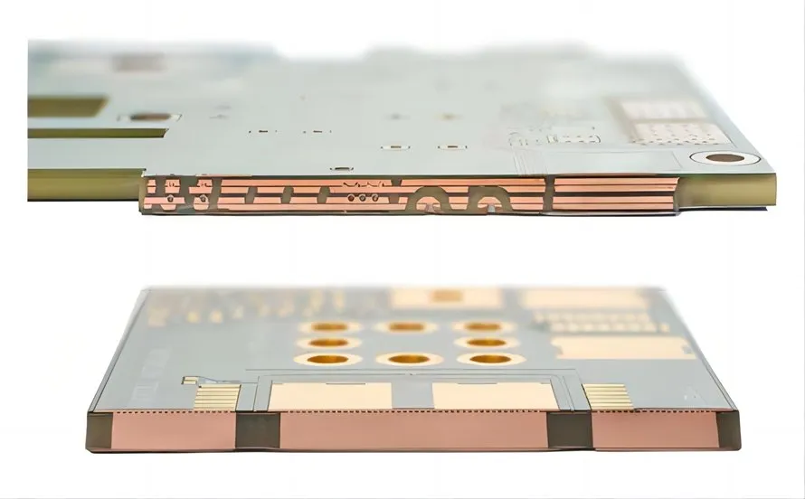
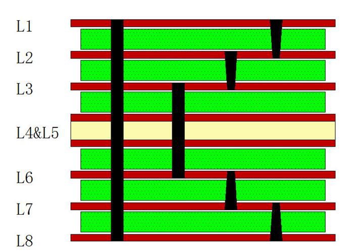
3. Layer Stack-Up Design for Signal Integrity
The layer stack-up in a sequential build-up PCB directly impacts sequential build-up PCB signal integrity. A well-designed stack-up ensures proper signal routing, reduces electromagnetic interference (EMI), and maintains impedance consistency across layers.
Consider these tips for optimizing your stack-up in high-frequency applications:
- Symmetrical Stack-Up: Design a balanced stack-up to prevent warping during manufacturing. For example, in a 10-layer SBU PCB, place power and ground planes symmetrically around the core.
- Ground Planes: Dedicate entire layers to ground planes near signal layers to provide a low-impedance return path. This reduces noise and crosstalk in high-frequency signals.
- Thin Dielectric Layers: Use thin dielectric layers (e.g., 2-4 mils) between signal and ground planes to tightly control impedance and reduce signal delay.
In RF designs, separating analog and digital signals across different layers can further enhance signal integrity. This minimizes interference between high-speed digital clocks and sensitive RF signals.
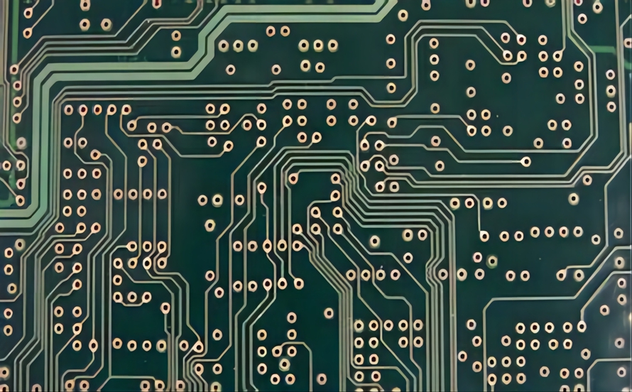
4. Minimizing Signal Loss and Crosstalk
Signal loss and crosstalk are major challenges in high-frequency PCB sequential build-up designs. At frequencies above 1 GHz, even small design flaws can lead to significant performance issues. Here's how to address these challenges:
- Smooth Copper Surfaces: Use smooth copper foils to reduce skin effect losses, where high-frequency signals travel only on the surface of conductors. Rough surfaces increase resistance and signal attenuation.
- Trace Routing: Avoid sharp bends in traces, as they cause signal reflections. Use 45-degree angles or curved traces instead. Maintain a minimum spacing of 3 times the trace width between adjacent high-speed lines to reduce crosstalk.
- Shielding: Incorporate shielding techniques, such as grounded guard traces or via fences, around sensitive RF lines to block interference.
Simulation tools can help predict and mitigate signal loss before manufacturing. By modeling your design at the intended operating frequency (e.g., 2.4 GHz for Wi-Fi applications), you can identify potential issues and adjust accordingly.
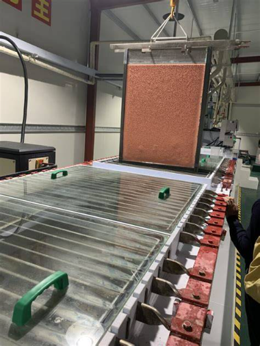
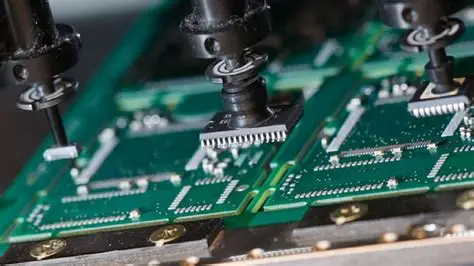
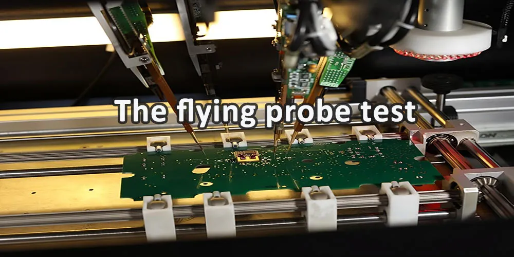
5. Manufacturing Precision for Sequential Build-Up PCBs
The manufacturing process for sequential build-up PCBs is more complex than for standard boards, especially for high-frequency applications. Precision is key to ensuring that the fine features and tight tolerances required for RF performance are achieved.
Key manufacturing considerations include:
- Microvia Reliability: Microvias, often with diameters as small as 4 mils, must be drilled and plated with high accuracy to avoid open circuits or signal discontinuities.
- Layer Registration: Misalignment between layers in an SBU design can disrupt impedance and signal paths. Tight registration tolerances, ideally within ±2 mils, are essential.
- Surface Finish: Choose a surface finish like immersion gold for RF boards to ensure low contact resistance and good signal transmission at high frequencies.
Partnering with a manufacturer experienced in SBU technology and high-frequency designs can make a significant difference in achieving the desired results.
Best Practices for High-Frequency PCB Design with Sequential Build-Up
Beyond the core considerations, adopting best practices can further enhance the performance of your sequential build-up PCBs in high-frequency applications. Here are some actionable tips:
- Simulation and Testing: Use electromagnetic simulation software to model signal behavior at your target frequency (e.g., 5 GHz for 5G applications). Validate the design with prototypes and testing equipment like vector network analyzers to measure insertion loss and return loss.
- Controlled Environment: High-frequency signals are sensitive to environmental factors like humidity and temperature. Design with these in mind, and consider protective coatings if the board will operate in harsh conditions.
- Component Placement: Place critical RF components close to their signal paths to minimize trace lengths. For example, keep RF amplifiers within 100 mils of their input/output lines to reduce parasitic effects.
Challenges in High-Frequency Sequential Build-Up PCB Design
While sequential build-up technology offers many advantages, it also comes with unique challenges in high-frequency applications. Understanding these hurdles can help you plan better:
- Cost: The advanced materials and precise manufacturing processes required for RF SBU PCBs often result in higher costs compared to standard designs.
- Design Complexity: Balancing impedance, signal integrity, and thermal management across multiple thin layers requires advanced tools and expertise.
- Manufacturing Limitations: Not all manufacturers can achieve the tight tolerances needed for high-frequency SBU designs, so choosing the right partner is critical.
Conclusion: Building Success with Sequential Build-Up PCBs
Designing sequential build-up PCBs for high-frequency applications is no small feat, but with the right approach, you can achieve outstanding results. By focusing on sequential build-up PCB signal integrity, mastering impedance control in sequential build-up, selecting the best sequential build-up materials for RF PCBs, and optimizing your high-frequency PCB sequential build-up design, you'll be well on your way to success.
Remember to prioritize precision in every aspect, from material selection to manufacturing. Use simulation tools to fine-tune your design, and work closely with experienced manufacturers to bring your vision to life. With these strategies, your high-frequency PCB projects will not only meet but exceed performance expectations, paving the way for innovation in RF and beyond.