ALLPCB


When it comes to assembling double-sided SMT (Surface Mount Technology) boards, choosing between wave soldering and reflow soldering is a critical decision. Both processes have unique strengths and limitations, especially for mixed technology assemblies or double-sided PCB designs. At a glance, reflow soldering is often the go-to for SMT components on double-sided boards due to its precision and compatibility with smaller components, while wave soldering excels for through-hole components and mixed assemblies. However, the right choice depends on your board design, component types, and production needs. In this comprehensive guide, we'll dive deep into the differences, limitations, and applications of wave soldering and reflow soldering for double-sided boards, helping you make an informed decision.
Understanding Double-Sided SMT Boards and Soldering Challenges
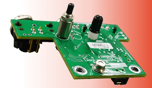
Double-sided SMT boards have components mounted on both sides of the PCB, maximizing space and functionality in compact designs. These boards are common in consumer electronics, automotive systems, and industrial applications. However, soldering components on both sides introduces challenges like thermal stress, component alignment, and the risk of damaging pre-soldered parts during secondary processes.
The primary goal of any soldering process is to create reliable electrical connections while avoiding defects like cold joints, tombstoning, or solder bridging. For double-sided boards, the process must also ensure that components on one side aren't affected when soldering the other. This is where the differences between wave soldering and reflow soldering become crucial, especially for mixed technology assemblies that combine SMT and through-hole components.
What Is Reflow Soldering and How Does It Work for Double-Sided SMT?
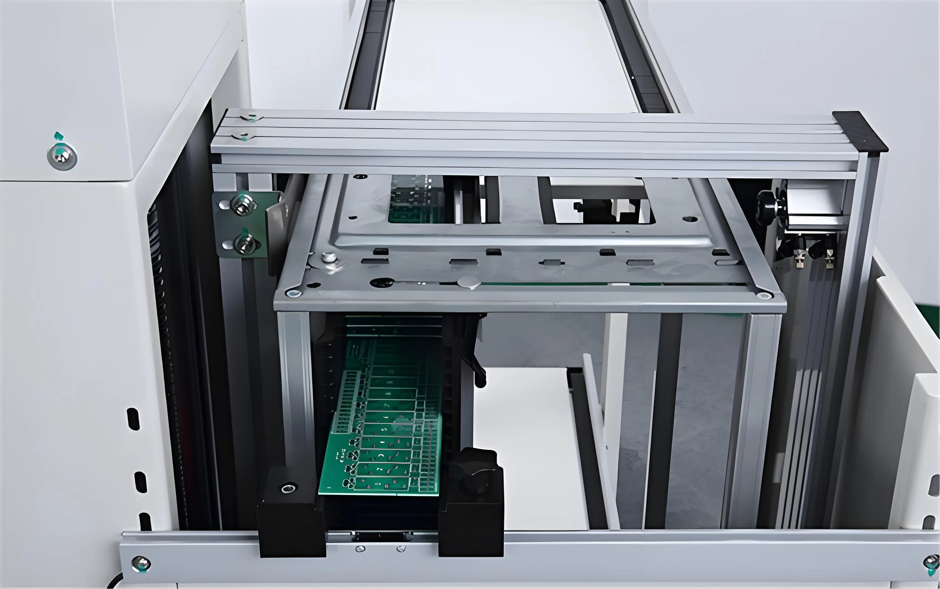
Reflow soldering is a process widely used for SMT components. It involves applying solder paste to the PCB, placing components, and then heating the board in a reflow oven. The heat melts the solder paste, forming strong connections as it cools. For double-sided SMT boards, reflow soldering is often performed in two passes: one for the bottom side and another for the top side.
In the first pass, the bottom-side components are soldered using a stencil to apply solder paste precisely. A low-temperature adhesive may be used to hold components in place during the second pass to prevent them from falling off due to gravity. The board then goes through the reflow oven again to solder the top-side components. Modern reflow ovens can reach temperatures of 220-260°C, depending on the solder alloy (e.g., lead-free SAC305), ensuring consistent melting across the board.
Advantages of Reflow Soldering for Double-Sided SMT
- Precision: Reflow soldering is ideal for small, densely packed SMT components (e.g., 0402 or 0201 packages) on double-sided boards, offering pinpoint accuracy.
- Consistency: The controlled heating profile minimizes thermal stress, reducing the risk of warping on double-sided PCBs.
- Automation: Fully automated pick-and-place machines and reflow ovens ensure high throughput for large-scale production.
Reflow Soldering Limitations for Double-Sided Boards
Despite its advantages, reflow soldering has limitations, especially for double-sided SMT designs and mixed technology assemblies. One key challenge is the risk of components on the bottom side reflowing again during the second pass, potentially causing misalignment or defects. To mitigate this, manufacturers often use adhesives or lower-temperature solder for the second pass, but this adds complexity and cost.
Additionally, reflow soldering struggles with through-hole components, which are common in mixed technology assemblies. The process isn't designed to fill through-hole vias with solder, often requiring a secondary soldering method like wave or selective soldering. For double-sided boards with a high mix of SMT and through-hole parts, relying solely on reflow can lead to incomplete joints or increased production time.
What Is Wave Soldering and Its Role in Double-Sided Boards?
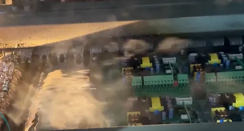
Wave soldering is a bulk soldering process primarily used for through-hole components. The PCB passes over a molten solder wave (typically at 250-260°C for lead-free solder), which wets the exposed leads and forms connections. While wave soldering isn't typically the first choice for double-sided SMT boards, it can be adapted for mixed technology assemblies where through-hole components are present on one side.
For double-sided boards, wave soldering is often used after reflow soldering to address through-hole components. The SMT components on the top side are soldered first via reflow, and then the board is flipped for wave soldering of through-hole parts on the bottom. However, SMT components on the bottom side must be masked or protected to avoid damage from the molten solder wave.
Advantages of Wave Soldering for Mixed Technology Assembly Double-Sided
- Speed: Wave soldering is faster for through-hole components, making it efficient for mixed technology assemblies with many pins to solder.
- Cost-Effective: It’s a less expensive process for high-volume production compared to manual soldering of through-hole parts.
- Reliability: Wave soldering creates strong, uniform joints for through-hole components, ideal for applications requiring durability.
Limitations of Wave Soldering for Double-Sided SMT
Wave soldering has significant limitations when applied to double-sided SMT boards. The process isn’t suitable for fine-pitch SMT components due to the risk of solder bridging and insufficient precision. For double-sided designs with SMT on both sides, wave soldering can damage or reflow bottom-side components unless they are protected with heat-resistant tape or fixtures, adding extra steps and costs.
Thermal shock is another concern. The rapid exposure to molten solder can stress the PCB and components, potentially causing cracks or delamination in double-sided boards with thin substrates (e.g., 0.8mm or less). This makes wave soldering less ideal for modern, compact designs with delicate SMT parts.
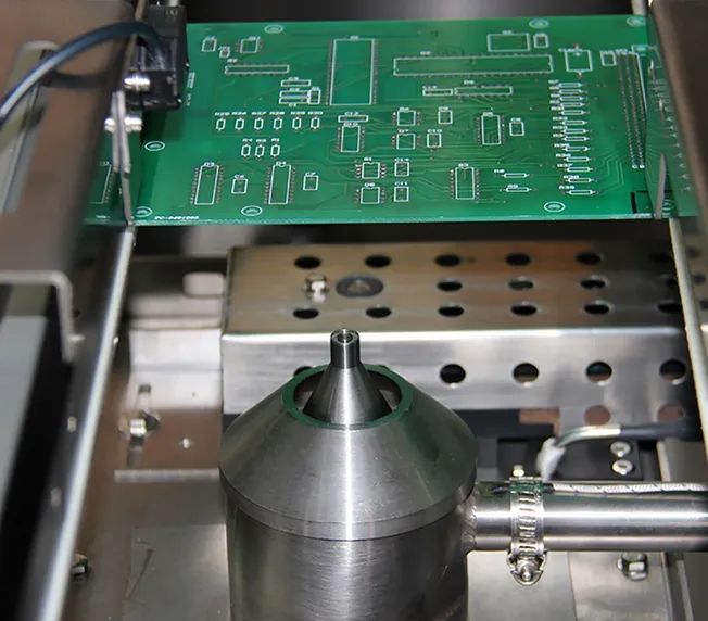
Selective Soldering for Double-Sided PCB: A Hybrid Solution
For double-sided PCBs with mixed technology or complex designs, selective soldering offers a middle ground between wave and reflow soldering. This process uses a precise nozzle to apply solder only to specific areas, typically for through-hole components, while avoiding SMT parts. Selective soldering is highly customizable, with programmable nozzles that can target exact locations on the board.
In double-sided PCB assembly, selective soldering is often used after reflow soldering to handle through-hole components without affecting SMT parts on either side. It minimizes thermal stress by limiting heat exposure to small areas, making it safer for delicate double-sided designs. For instance, selective soldering can achieve joint formation in as little as 2-5 seconds per pin, compared to the broader exposure of wave soldering.
Benefits of Selective Soldering for Double-Sided PCB
- Precision: Targets specific through-hole joints without impacting nearby SMT components.
- Flexibility: Ideal for mixed technology assemblies on double-sided boards with varying component types.
- Reduced Thermal Stress: Localized heating prevents damage to pre-soldered SMT parts or thin PCB substrates.
Drawbacks of Selective Soldering
While selective soldering is versatile, it’s slower than wave soldering for high-volume production due to its point-by-point approach. The equipment is also more expensive and requires skilled programming to ensure accuracy. For double-sided SMT boards with minimal through-hole components, the added cost and time may not be justified compared to reflow soldering alone.
Comparing Wave Soldering and Reflow for Double-Sided Boards
To choose the right process for your double-sided SMT or mixed technology assembly, consider the following factors:
Component Types
- Reflow Soldering: Best for SMT components on both sides of the board, especially fine-pitch parts (e.g., pitch below 0.5mm).
- Wave Soldering: Suited for through-hole components in mixed assemblies but risky for SMT on the bottom side.
- Selective Soldering: Ideal for mixed technology double-sided boards with a combination of SMT and through-hole parts.
Production Volume
- Reflow Soldering: Efficient for high-volume SMT production with automated lines.
- Wave Soldering: Faster for through-hole components in large batches but less adaptable for SMT.
- Selective Soldering: Slower and better for low-to-medium volume or prototypes with complex designs.
Board Complexity
- Reflow Soldering: Handles complex, densely populated double-sided SMT boards with ease.
- Wave Soldering: Struggles with dense SMT layouts due to lack of precision and thermal risks.
- Selective Soldering: Adapts well to complex mixed technology assemblies on double-sided PCBs.
Cost Considerations
- Reflow Soldering: Higher initial setup costs for equipment and adhesives but cost-effective for SMT-heavy designs.
- Wave Soldering: Lower equipment costs but may require additional masking or protection for double-sided SMT.
- Selective Soldering: Higher equipment and programming costs, best for specialized applications.
Best Practices for Double-Sided SMT Soldering
Regardless of the soldering method you choose, following best practices can improve outcomes for double-sided boards:
- Design for Manufacturability (DFM): Place heavier or heat-sensitive components on the top side to minimize risks during secondary soldering passes.
- Thermal Profiling: Use precise temperature profiles (e.g., peak at 245°C for lead-free solder) in reflow ovens to avoid overheating double-sided boards.
- Component Spacing: Ensure adequate spacing (at least 0.3mm) between fine-pitch SMT components to prevent solder bridging in reflow or wave soldering.
- Protective Measures: Use heat-resistant tape or fixtures to shield bottom-side SMT components during wave soldering.
Conclusion: Making the Right Choice for Your Double-Sided Boards
Choosing between wave soldering and reflow soldering for double-sided SMT boards depends on your specific project requirements. Reflow soldering shines for SMT-heavy designs, offering precision and consistency for fine-pitch components on both sides. However, its limitations with through-hole parts may require a secondary process. Wave soldering is efficient for mixed technology assemblies with through-hole components but poses challenges for double-sided SMT due to thermal risks and lack of precision. For complex designs, selective soldering provides a tailored solution, balancing precision and flexibility at a higher cost.
By understanding the strengths and limitations of each method—whether it's wave soldering for double-sided SMT, reflow soldering limitations, mixed technology assembly double-sided, or selective soldering for double-sided PCB—you can optimize your assembly process. Evaluate your board design, component mix, and production goals to select the best approach, ensuring high-quality, reliable results for your electronic products.