 ALLPCB


In the world of printed circuit board (PCB) manufacturing, the solder mask is a critical yet often underappreciated component. This thin polymer layer protects copper traces, prevents solder bridges, and ensures the long-term reliability of electronic devices. However, achieving a durable and effective solder mask requires precision, the right materials, and adherence to best practices. In this comprehensive guide, we explore the key considerations for solder mask application, offering actionable insights for engineers to optimize PCB durability and performance.
What Is a Solder Mask and Why Does It Matter?
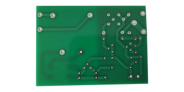
A solder mask, also known as solder resist, is a protective polymer coating applied to the copper traces of a PCB. Its primary functions are to prevent oxidation, insulate conductive paths to avoid short circuits, and protect the board from environmental factors like moisture, dust, and chemicals. By covering areas where soldering is not required, the solder mask ensures precise solder joint formation during assembly, reducing defects like solder bridges—unintended connections caused by excess solder.
The importance of a properly applied solder mask cannot be overstated. For instance, in high-reliability applications such as medical devices or aerospace electronics, a durable solder mask ensures consistent performance under demanding conditions. Poor application can lead to issues like mask peeling, undercuring, or insufficient coverage, compromising the PCB's longevity and functionality.
Types of Solder Masks and Their Applications
Choosing the right solder mask type is crucial for durability and performance. The main types of solder masks include:
1. Epoxy Liquid Solder Mask
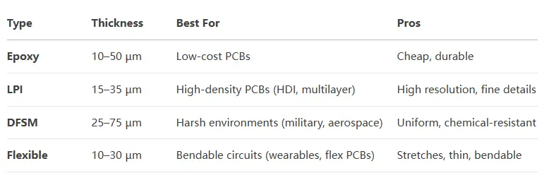
- Description: This is the most cost-effective option, applied via silkscreen printing. It uses a thermosetting epoxy that hardens during thermal curing.
- Applications: Suitable for single- or double-sided PCBs with simpler designs. It offers good chemical resistance but less precision for high-density boards.
- Pros: Low cost, easy to apply.
- Cons: Limited precision for fine-pitch components.
2. Liquid Photoimageable Solder Mask (LPI)
- Description: LPI is a photosensitive liquid applied via screen printing, spray, or curtain coating, then exposed to UV light to create precise patterns. It's the most common type in modern PCB manufacturing.
- Applications: Ideal for multilayer PCBs and high-density interconnects (HDI) due to its precision and durability.
- Pros: High accuracy, strong adhesion, durable epoxy-based composition.
- Cons: Requires careful curing to avoid undercuring issues.
Suggested Reading: Comprehensive Introduction to LPI Solder Mask in PCB Manufacturing
3. Dry Film Photoimageable Solder Mask (DFSM)
- Description: DFSM is a pre-formed photosensitive film laminated onto the PCB surface, then exposed and developed. It provides uniform thickness across large areas.
- Applications: Best for high-volume production or boards requiring thick solder mask layers, such as the heavy copper PCB.
- Pros: Consistent thickness, cost-effective for large-scale manufacturing.
- Cons: Less effective for complex surface topographies.
Suggested Reading: Dry Film Solder Mask vs. Liquid Photoimageable (LPI): Which is Best for Your PCB Project
4. Flexible Solder Mask (for Flex PCBs)
- Description: Formulated to withstand bending and flexing, these masks are thinner (10–30 microns) and applied via screen printing or photolithography.
- Applications: Used in flexible and rigid-flex PCBs for wearables or space-constrained devices.
- Pros: High flexibility, suitable for dynamic applications.
- Cons: Higher cost and complex application process.
Best Practices for Solder Mask Application
To ensure a durable solder mask that enhances PCB reliability, follow these best practices during design, material selection, and application.
1. Optimize Solder Mask Design
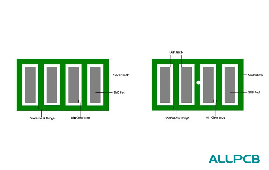
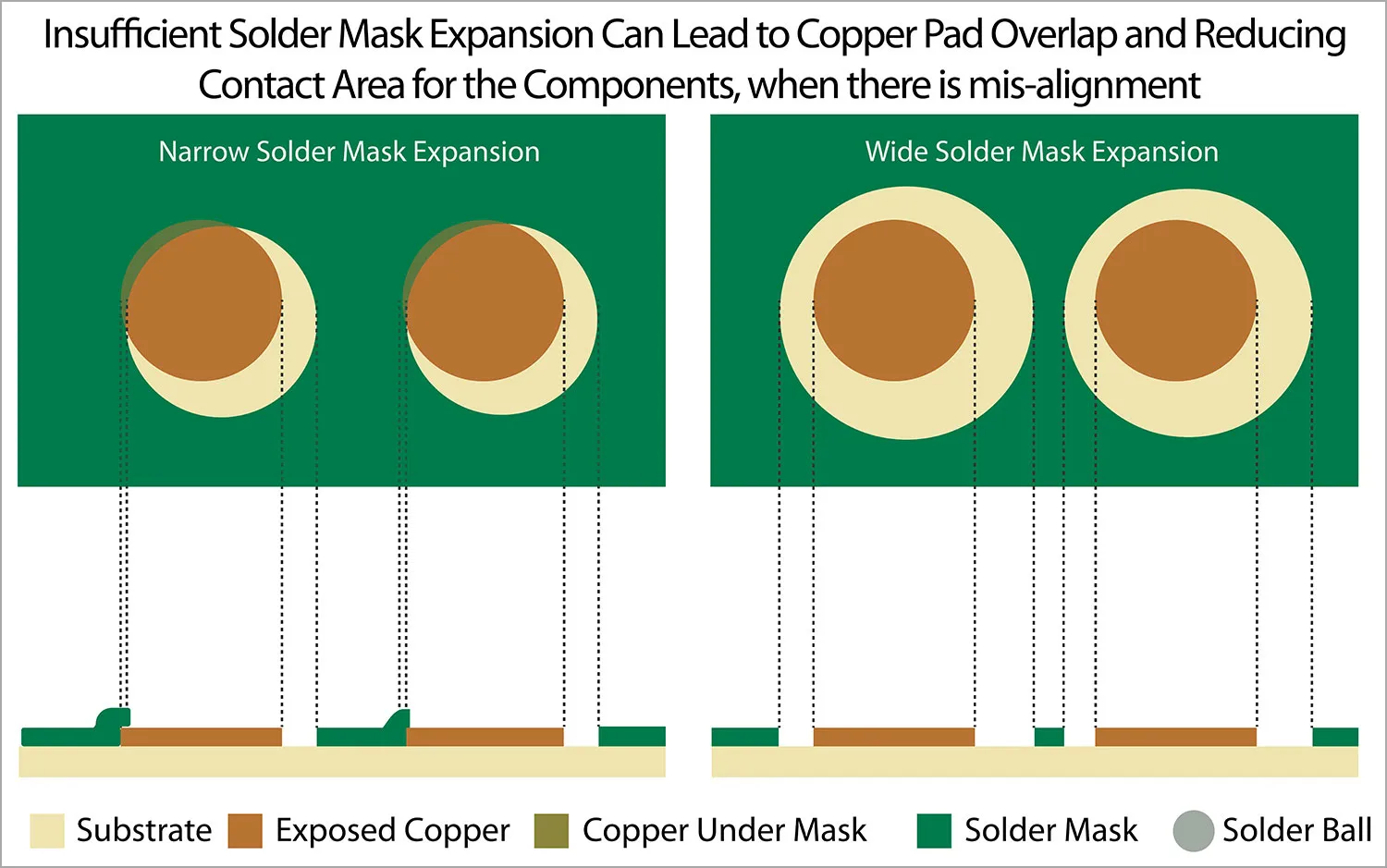
- Solder Mask Clearances: Maintain a minimum clearance of 1.6–2 mil between solder mask edges and surface-mount technology (SMT) pads to prevent mask encroachment, which can cause weak solder joints. For example, a typical solder mask aperture should be 4 mil larger than the copper pad (2 mil per side) to account for registration tolerances of ±2 mil.
- Solder Mask Dams: Include dams (minimum 8 mil for 1 oz copper, 10 mil for 2 oz copper) between fine-pitch pads to prevent solder bridges. For non-green masks, add an extra 1 mil to ensure adhesion.
- Via Tenting: Tent or plug vias near SMT pads to prevent solder starvation, where solder wicks away from pads into open vias, causing poor connections.
- Design Rule Checks (DRC): Run DRCs to verify clearances, dam dimensions, and aperture sizes. Ensure your design aligns with your contract manufacturer's (CM) capabilities.
2. Choose the Right Solder Mask Material
- Match Material to Application: For high-reliability applications (e.g., military or medical), use LPI masks for their durability and precision. For cost-sensitive projects, epoxy liquid masks suffice for simpler boards.
- Consider Environmental Factors: Select materials with high chemical resistance and thermal stability, such as Taiyo solder mask inks, which offer excellent heat resistance for heavy copper PCBs.
- Flexibility for Flex PCBs: For flexible circuits, choose a solder mask that can withstand bending without cracking, adhering to IPC-SM-840C standards for durability and adhesion.
Suggested Reading: Solder Mask Materials for High-Frequency PCBs: Minimizing Signal Loss
3. Ensure Proper Application Techniques
- Surface Preparation: Clean the PCB thoroughly to remove contaminants like dust or flux residues, which can cause poor adhesion or undercuring.
- Application Methods:
- Silkscreen Printing: Best for epoxy liquid masks on simpler boards. Ensure even ink distribution to avoid uneven thickness.
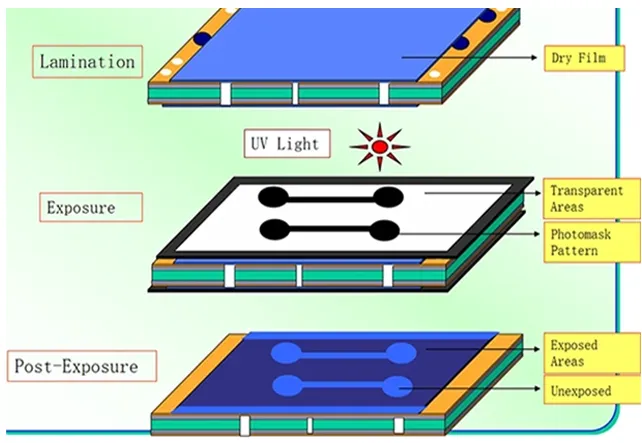
- Photoimaging (LPI): Use UV exposure with a high-quality photomask for precision. Verify exposure energy to prevent undercuring, which leaves the mask tacky and prone to peeling.
- Dry Film Lamination (DFSM): Vacuum laminate DFSM to ensure uniform thickness, especially for heavy copper PCBs with copper thickness >3 oz.
- Curing Process: Use appropriate curing conditions (e.g., UV light, heat, or a combination) based on the mask type. For LPI, curing typically requires 150–200°C for 30–60 minutes. Undercuring can reduce durability, while overcuring may cause brittleness.
4. Address Challenges in Heavy Copper and HDI Boards
- Heavy Copper PCBs: These boards (copper thickness >3 oz) pose challenges due to high thermal conductivity and surface height differences. Use multiple thin layers of LPI or DFSM to ensure coverage without cracking. For example, apply a base layer to fill substrate gaps before standard printing.
- HDI PCBs: High-density interconnect boards require precise solder mask application to avoid small openings or misalignment. Use laser direct imaging (LDI) with LPI masks for better precision, achieving registration accuracies of ±50 μm.
- Thermal Management: Ensure the solder mask can withstand reflow soldering temperatures (up to 260°C) without degrading. Test for thermal cycling resilience to prevent cracking during operation.
5. Adhere to Industry Standards
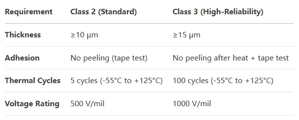
- IPC-SM-840C: Follow this standard for solder mask qualification, covering durability, adhesion, and thickness requirements. For high-reliability applications (Class 3), ensure the mask meets stringent performance criteria.
- NCAB Group Specifications: For critical applications, adopt additional requirements like NCAB's 70% via hole fill to enhance reliability in harsh environments.
- Solder Mask Thickness: Aim for 10–30 microns for standard PCBs and 15–50 microns for heavy copper boards. Avoid excessive thickness, which can interfere with fine-pitch component placement.
Common Solder Mask Errors and How to Avoid Them
Even with careful planning, solder mask application can go wrong. Here are common issues and solutions:
- Insufficient Clearance: Small clearances (<1.6 mil) can cause mask encroachment on pads, leading to weak solder joints. Solution: Expand apertures by 4 mil and run DRCs.
- Undercuring: Tacky or soft masks result from inadequate UV exposure or heat. Solution: Optimize curing parameters (e.g., 150°C for 45 minutes for LPI) and test adhesion post-curing.
- Misregistration: Misaligned masks expose copper or cover pads. Solution: Use advanced registration techniques like LDI and maintain tolerances of ±50 μm.
- Cracking or Peeling: Common in heavy copper PCBs due to thermal stress. Solution: Use flexible, high-adhesion masks and apply multiple thin layers.
- Incomplete Via Tenting: Open vias can cause solder starvation. Solution: Tent or plug vias with solder mask or resin to ensure coverage.
How ALLPCB Supports Solder Mask Application
At ALLPCB, we understand the critical role of solder mask application in ensuring PCB durability. Our advanced manufacturing capabilities, including state-of-the-art LDI equipment and adherence to IPC-SM-840C standards, enable us to deliver precise and reliable solder mask application for both standard and complex PCBs. Whether you need quick-turn prototyping for HDI designs or high-volume production for heavy copper boards, our global logistics and expertise ensure your PCBs meet the highest quality standards. Contact us at ALLPCB.com to streamline your PCB manufacturing process with tailored solutions.
Conclusion
A durable solder mask is essential for protecting PCBs from environmental damage, preventing solder bridges, and ensuring long-term reliability. By optimizing design, selecting the right materials, applying precise techniques, and adhering to industry standards, engineers can significantly enhance PCB performance. From choosing LPI for high-density boards to addressing challenges in heavy copper designs, these best practices provide a roadmap for success. With careful attention to detail and collaboration with a trusted manufacturer, you can achieve robust, high-quality PCBs that stand the test of time.





