ALLPCB


In the fast-paced world of gaming, every millisecond counts. For gaming console designers, ensuring top-notch signal integrity in printed circuit board (PCB) design is the key to minimizing latency and delivering a seamless user experience. Whether you're working on high-speed PCB design for gaming consoles or tackling issues like crosstalk and impedance mismatches, understanding signal integrity can make or break performance. In this blog, we’ll uncover the secrets to optimizing gaming console PCB signal integrity, focusing on practical techniques for impedance matching, crosstalk reduction, and signal integrity simulation.
Dive into this comprehensive guide to learn actionable strategies that reduce latency and boost performance in gaming hardware. From understanding the basics of signal integrity to applying advanced design practices, we’ve got you covered with detailed insights and tips tailored for engineers and designers in the gaming industry.
Why Signal Integrity Matters in Gaming Console PCB Design
Signal integrity refers to the quality of an electrical signal as it travels through a PCB. In gaming consoles, where high-speed data transfer is critical, poor signal integrity can lead to latency, data errors, and degraded performance. Modern consoles handle massive amounts of data between processors, memory, and peripherals, often at speeds exceeding 10 Gbps. Any disruption in signal quality can result in delays that frustrate gamers or cause system glitches.
For instance, a poorly designed PCB might introduce signal delays of several nanoseconds per trace, which can accumulate and impact gameplay responsiveness. By prioritizing gaming console PCB signal integrity, designers ensure that signals remain clean, fast, and reliable, directly contributing to a better gaming experience.

Key Challenges in High-Speed PCB Design for Gaming Consoles
Designing PCBs for gaming consoles comes with unique challenges due to the need for high-speed data transmission in a compact form factor. Let’s explore the primary obstacles engineers face and how they relate to signal integrity.
1. Latency and Signal Propagation Delay
Latency is the time it takes for a signal to travel from its source to its destination. In gaming consoles, even a delay of 1-2 nanoseconds can affect real-time performance, especially in competitive gaming. Signal propagation delay is influenced by trace length, dielectric material properties, and routing inefficiencies. The longer the trace, the greater the delay, which is why minimizing trace lengths is a priority in high-speed PCB design for gaming consoles.
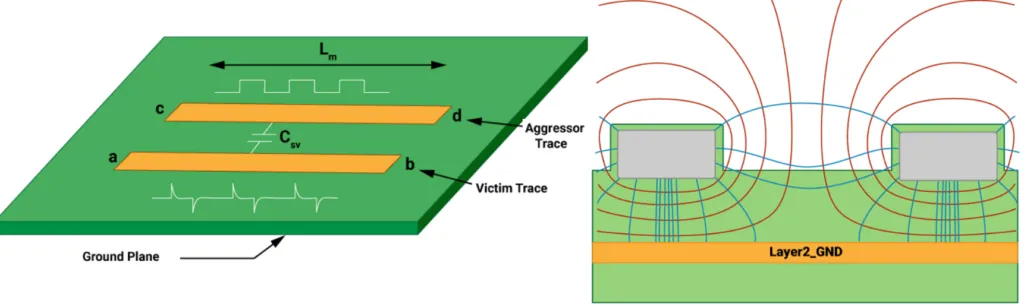
2. Crosstalk Between Traces
Crosstalk occurs when signals from adjacent traces interfere with each other, causing noise and potential data errors. In densely packed gaming console PCBs, where space is limited, traces often run close together, increasing the risk of crosstalk. This interference can degrade signal quality, leading to slower response times and glitches.
3. Impedance Mismatches
Impedance matching in gaming PCBs ensures that signals transfer efficiently between components without reflection or loss. A mismatch, such as a trace with an impedance of 60 ohms connected to a component expecting 50 ohms, can cause signal reflections, leading to data corruption and increased latency. Proper impedance control is essential for maintaining signal integrity at high speeds.
Strategies for Minimizing Latency in Gaming Console PCB Design
Now that we’ve identified the challenges, let’s dive into practical strategies to optimize gaming console PCB signal integrity and reduce latency. These techniques are tailored for high-speed PCB design and focus on real-world applications.
1. Optimize Trace Routing for Shorter Paths
One of the simplest ways to reduce latency is by minimizing the length of signal traces. Shorter traces mean less propagation delay, as signals have less distance to travel. For example, a signal traveling through a 10-inch trace on a standard FR-4 material might experience a delay of around 1.5 nanoseconds, while a 5-inch trace cuts that delay in half.
To achieve this, plan your PCB layout to place high-speed components, like GPUs and memory modules, as close together as possible. Use direct routing paths and avoid unnecessary loops or detours. Additionally, consider using differential pairs for critical signals, as they maintain consistent timing and reduce noise.
2. Implement Impedance Matching in Gaming PCBs
Impedance matching is a cornerstone of signal integrity in high-speed designs. To prevent signal reflections, ensure that the impedance of traces matches the impedance of connected components. For instance, many high-speed interfaces in gaming consoles, such as DDR memory or PCIe lanes, require a characteristic impedance of 50 ohms.
Achieve this by carefully calculating trace width and spacing based on the dielectric constant of your PCB material. Use PCB design software with built-in impedance calculators to maintain consistency. If mismatches occur, consider adding termination resistors to absorb reflected signals and stabilize the system.
3. Crosstalk Reduction in Gaming Console PCBs
Reducing crosstalk is vital for maintaining clean signals in compact gaming console layouts. Start by increasing the spacing between high-speed traces. A general rule of thumb is to keep traces at least three times the trace width apart to minimize electromagnetic interference (EMI).
Another effective method is to use ground planes between signal layers. A solid ground plane acts as a shield, absorbing stray electromagnetic fields and preventing crosstalk. For critical signals, consider routing them on separate layers or using guard traces—grounded traces placed between signal lines—to further isolate them.
4. Leverage Signal Integrity Simulation for PCB Design
Before manufacturing a gaming console PCB, use signal integrity simulation tools to predict and address potential issues. These simulations analyze factors like signal delay, crosstalk, and impedance mismatches, allowing you to fine-tune your design virtually. For example, simulation software can model a high-speed signal at 10 Gbps and identify areas where reflections exceed acceptable thresholds, such as 5% of the signal amplitude.
Running simulations early in the design process saves time and reduces costly redesigns. Many modern PCB design platforms offer integrated simulation features, making it easier to test different layouts and configurations for optimal performance.
Advanced Techniques for High-Speed PCB Design in Gaming Consoles
Beyond the basics, advanced design techniques can further enhance gaming console PCB signal integrity. These methods are particularly useful for cutting-edge consoles pushing the boundaries of speed and performance.
1. Use High-Quality Dielectric Materials
The choice of PCB material significantly impacts signal integrity. Standard FR-4 materials work for lower-speed designs but may introduce higher signal loss at frequencies above 5 GHz, common in modern gaming hardware. Instead, opt for low-loss materials like Rogers or Isola, which have lower dielectric constants (around 3.0-3.5 compared to FR-4’s 4.5) and better signal transmission properties.
While these materials cost more, they reduce signal attenuation and delay, ensuring faster data transfer and lower latency for gamers.
2. Adopt Via Optimization Techniques
Vias, the connections between PCB layers, can introduce signal delays and impedance discontinuities if not designed carefully. In high-speed PCB design for gaming consoles, minimize the number of vias on critical signal paths. When vias are necessary, use back-drilling to remove unused via stubs, which can cause signal reflections.
Additionally, ensure via diameters and pad sizes are optimized for the signal frequency. Smaller vias reduce parasitic capacitance, improving signal quality at high speeds.
3. Implement Power Integrity Alongside Signal Integrity
Signal integrity and power integrity go hand in hand. Voltage fluctuations or noise in the power delivery network (PDN) can degrade signal quality, leading to increased latency. Use decoupling capacitors near high-speed components to stabilize voltage levels and reduce noise. For example, placing a 0.1 μF capacitor within 0.1 inches of a processor pin can effectively filter out high-frequency noise.
Design a robust PDN with low-impedance paths to ensure clean power delivery, supporting overall signal integrity in the system.
Common Mistakes to Avoid in Gaming Console PCB Design
Even experienced engineers can overlook critical details in high-speed PCB design. Here are common pitfalls to avoid when optimizing gaming console PCB signal integrity.
1. Ignoring Ground Plane Integrity
A fragmented or poorly designed ground plane can lead to increased noise and crosstalk. Ensure a continuous, unbroken ground plane beneath high-speed traces to provide a stable return path for signals. Avoid splitting ground planes unless absolutely necessary for isolation purposes.
2. Neglecting Signal Layer Stacking
In multi-layer PCBs, improper layer stacking can exacerbate signal integrity issues. Place high-speed signal layers adjacent to ground planes to minimize loop inductance and EMI. Avoid routing high-speed signals on outer layers exposed to external interference.
3. Overlooking Thermal Management
Gaming consoles generate significant heat, which can affect signal integrity by altering material properties and trace resistance. Integrate thermal vias and heat sinks into your design to dissipate heat effectively, ensuring consistent signal performance under load.
Conclusion: Building Faster, More Reliable Gaming Consoles
Signal integrity is the backbone of high-performance gaming console PCB design. By focusing on techniques like impedance matching, crosstalk reduction, and signal integrity simulation, engineers can minimize latency and deliver an unparalleled gaming experience. From optimizing trace routing to selecting advanced materials, every design decision plays a role in ensuring signals travel quickly and cleanly through the board.
At the heart of successful high-speed PCB design for gaming consoles lies a commitment to precision and foresight. By adopting the strategies outlined in this guide, you can overcome common challenges and build hardware that meets the demands of modern gamers. Start implementing these signal integrity secrets today to create gaming consoles that stand out for their speed, reliability, and performance.