 ALLPCB


In the world of financial transactions, security is everything. If you're designing hardware for payment systems, you might be wondering how to create a PCB layout that meets EMV compliance while ensuring top-notch protection against tampering and data theft. The answer lies in following strict EMV PCB design guidelines, integrating secure elements, and applying PCB security best practices tailored for financial transaction hardware.
In this comprehensive guide, we'll walk you through the essential strategies for designing secure financial hardware. From anti-tampering PCB design to secure element integration, we’ll cover actionable tips and detailed insights to help you build robust and compliant systems. Whether you're an engineer or a hardware designer, this blog will equip you with the knowledge to create reliable and secure PCB layouts for financial applications.
Understanding EMV Compliance and Its Impact on PCB Design
EMV, which stands for Europay, Mastercard, and Visa, is a global standard for secure payment transactions using smart chip technology. It was developed to reduce fraud in card-based transactions by replacing magnetic stripe cards with more secure chip-enabled cards. For hardware designers, EMV compliance means adhering to strict guidelines that ensure the security and integrity of financial transactions at the hardware level.
When designing a PCB for EMV-compliant hardware, the layout must prioritize data protection, signal integrity, and resistance to physical and electronic attacks. This involves careful planning of component placement, trace routing, and shielding to prevent unauthorized access to sensitive information. Non-compliance can lead to vulnerabilities, failed certifications, and costly redesigns, making it critical to get the design right from the start.
Key EMV PCB Design Guidelines for Financial Hardware
Creating a PCB layout for EMV compliance requires attention to several key factors. Below are the essential guidelines to follow for a secure and compliant design.
1. Optimize Component Placement for Security
The placement of components on a PCB for financial hardware must minimize the risk of tampering and interception. Place sensitive components, such as secure elements or microcontrollers, in areas that are hard to access. For example, position them away from board edges and cover them with protective layers or enclosures. Additionally, keep critical components close together to reduce trace lengths and minimize the risk of signal interception.
A practical tip is to place the secure element near the center of the PCB, surrounded by other non-critical components as a physical barrier. This setup can deter attackers attempting to probe or modify the hardware. Also, ensure that power and ground pins are directly connected to their respective planes with minimal trace exposure to reduce electromagnetic interference (EMI) risks.
2. Implement Robust Grounding and Shielding
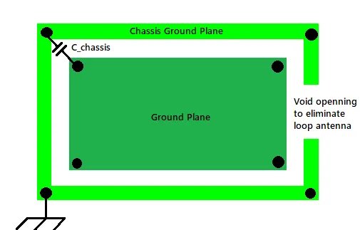
Grounding is a cornerstone of PCB security best practices, especially for financial transaction PCB layouts. A solid ground plane helps reduce noise and provides a stable reference for sensitive signals. For EMV-compliant designs, use a continuous ground plane across the entire PCB to prevent ground loops and ensure low impedance paths for return currents. A typical impedance target for high-speed signals in financial hardware is around 50 ohms, which helps maintain signal integrity.
Shielding is equally important. Use metal enclosures or conductive coatings around sensitive areas of the PCB to block electromagnetic fields that could be exploited to extract data. For example, a Faraday cage-like structure around the secure element can prevent radio frequency (RF) attacks. Ensure that the shield is properly grounded to avoid creating unintended antennas that could worsen EMI issues.
3. Secure Trace Routing for Data Protection
Trace routing plays a vital role in protecting sensitive data on a financial transaction PCB layout. Avoid running critical traces, such as those connected to the secure element or cryptographic modules, on outer layers of the PCB where they can be easily probed. Instead, route them on inner layers sandwiched between ground planes to provide natural shielding.
Additionally, maintain consistent trace widths and spacing to avoid impedance mismatches. For high-speed signals like those in EMV card readers (often operating at speeds up to 12 MHz), a trace width of 6-8 mils with a spacing of at least 10 mils can help maintain signal integrity and reduce crosstalk. Use differential pair routing for clock and data lines to further minimize noise and ensure reliable communication.
PCB Security Best Practices for Financial Transaction Hardware
Beyond EMV-specific guidelines, there are broader PCB security best practices that enhance the overall protection of financial hardware. These practices focus on preventing unauthorized access, detecting tampering, and ensuring data integrity.
1. Anti-Tampering PCB Design Techniques
Anti-tampering PCB design is critical for financial hardware, as attackers often attempt to physically access or modify the board to steal sensitive data like PINs or cryptographic keys. One effective technique is to use tamper-detection circuits that trigger an alarm or wipe sensitive data if unauthorized access is detected. For instance, integrate micro-switches or conductive mesh layers around the PCB that break if the board is physically altered.
Another approach is to use epoxy potting or conformal coatings over sensitive areas of the PCB. These materials make it difficult to remove components or probe traces without damaging the hardware. Some designs even incorporate self-destruct mechanisms, such as fuses that burn out critical circuits if tampering is detected, rendering the device unusable.
2. Secure Power Supply Design
The power supply circuitry in financial hardware can be a weak point if not designed with security in mind. Attackers may use power analysis attacks, such as differential power analysis (DPA), to extract cryptographic keys by monitoring power consumption fluctuations. To counter this, incorporate power filters and decoupling capacitors near sensitive components to smooth out power variations. A common practice is to use capacitors with values of 0.1 μF to 1 μF placed within 100 mils of power pins.
Additionally, consider implementing randomized power consumption techniques or dummy operations in the firmware to obscure power usage patterns. This makes it harder for attackers to correlate power spikes with specific operations like encryption or decryption.
3. Minimize External Interfaces
Every external interface on a financial transaction PCB is a potential entry point for attacks. Limit the number of exposed ports, debug interfaces, and test points on the board. If debug ports are necessary during development, ensure they are disabled or physically removed in the final production version. Use encrypted communication protocols for any external connections to prevent data interception.
For example, if a USB interface is required for firmware updates, secure it with strong authentication mechanisms to prevent unauthorized access. Additionally, place protective diodes or resistors on interface lines to guard against voltage spikes or reverse engineering attempts.
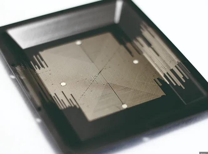
Secure Element Integration in PCB Design
A secure element (SE) is a tamper-resistant hardware module that stores sensitive data, such as cryptographic keys and user credentials, in financial hardware. Integrating a secure element into your PCB design is a cornerstone of EMV compliance and overall security.
1. Placement and Isolation of Secure Elements
Place the secure element in a location that minimizes exposure to physical and electronic attacks. As mentioned earlier, positioning it in the center of the PCB, surrounded by other components, adds a layer of protection. Electrically isolate the secure element by using dedicated power and ground connections that are separate from other parts of the circuit. This reduces the risk of side-channel attacks through shared power lines.
2. Secure Communication with the Secure Element
Communication between the secure element and other components, such as the main microcontroller, must be encrypted and protected. Use secure protocols like I2C or SPI with hardware-based encryption to prevent eavesdropping. Route communication traces on inner layers and keep them as short as possible—ideally under 500 mils—to reduce the chance of interception.
Additionally, implement hardware-based access controls to ensure that only authorized components can interact with the secure element. For instance, use a dedicated bus with access restricted through firmware to block unauthorized commands.
Testing and Validation for EMV Compliance
Once your PCB design is complete, rigorous testing and validation are essential to ensure it meets EMV standards and provides the required level of security. Conduct signal integrity tests to verify that data transmission between the card reader and the secure element operates within specified parameters, such as maintaining a bit error rate (BER) below 10^-6.
Perform penetration testing to identify vulnerabilities in the hardware. This includes attempting physical tampering, power analysis, and RF attacks to see if sensitive data can be extracted. Work with certified testing labs to validate compliance with EMVCo standards, which include specific requirements for terminal security and transaction processing.
Finally, ensure that your design adheres to other relevant standards, such as PCI DSS (Payment Card Industry Data Security Standard), which often overlaps with EMV requirements for financial hardware. Addressing these standards during the design phase can save time and resources during certification.
Common Challenges in Financial Transaction PCB Layout
Designing a PCB for financial hardware comes with unique challenges. One common issue is balancing security with manufacturability. Adding multiple layers for shielding or tamper-detection meshes can increase production costs and complexity. To mitigate this, collaborate with your manufacturing partner early in the design process to identify cost-effective solutions without compromising security.
Another challenge is managing heat dissipation in compact designs. Secure elements and cryptographic processors often generate significant heat, which can affect performance if not addressed. Use thermal vias and heat sinks strategically placed near high-power components to manage temperatures, ensuring they stay within safe limits (typically below 85°C for most ICs).
Conclusion: Building Trust Through Secure PCB Design
Designing secure financial hardware is a complex but critical task. By following EMV PCB design guidelines, implementing PCB security best practices, and focusing on anti-tampering PCB design and secure element integration, you can create robust hardware that protects sensitive data and meets global standards. A well-designed financial transaction PCB layout not only ensures compliance but also builds trust with users and stakeholders in an industry where security is non-negotiable.
Start with a clear plan, prioritize security at every stage, and leverage the strategies outlined in this guide to achieve a reliable and compliant design. With the right approach, your hardware can stand up to the challenges of modern payment systems and contribute to a safer financial ecosystem.


