ALLPCB


If you're dealing with challenges in thick copper PCB manufacturing, you're not alone. Issues like uneven etching, plating defects, delamination, stackup errors, and misalignment can disrupt production and affect board performance. In this detailed guide, we'll walk you through the most common problems and provide practical solutions for etching, plating, delamination, stackup, and alignment issues. Whether you're an engineer or a manufacturer, you'll find actionable tips to improve your process and ensure high-quality results.
Introduction to Thick Copper PCB Manufacturing Challenges
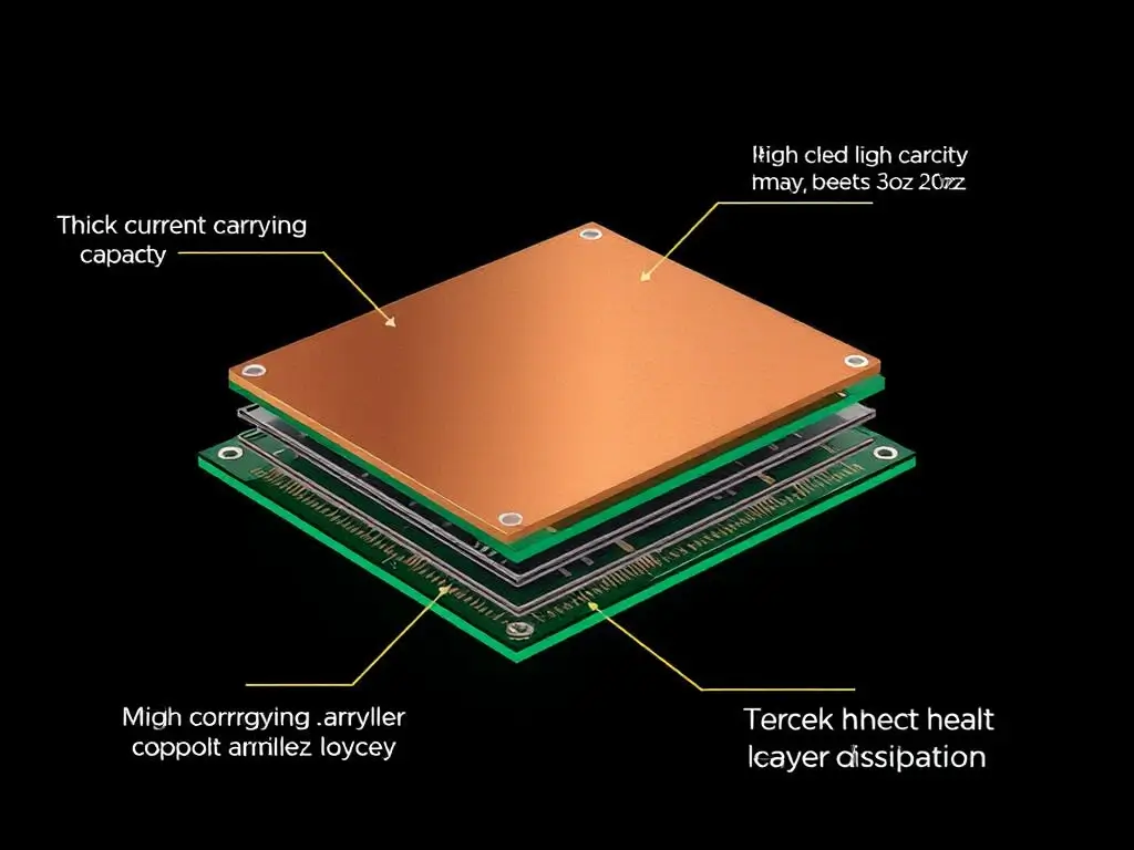
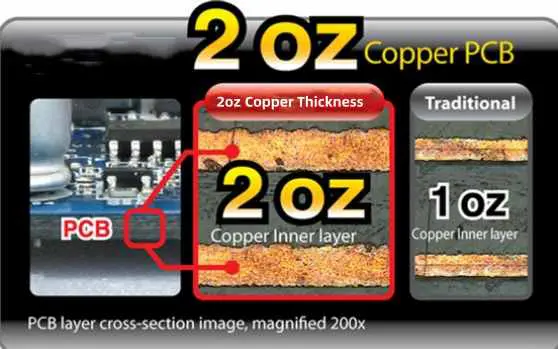
Thick copper PCBs are essential for high-power applications, such as power electronics, automotive systems, and industrial equipment. These boards often feature copper layers thicker than 3 oz/ft2 (105 μm), sometimes reaching up to 20 oz/ft2 (700 μm) or more. While thick copper offers excellent thermal management and current-carrying capacity, it also introduces unique manufacturing challenges. Etching precision, plating uniformity, layer adhesion, stackup design, and alignment accuracy are just a few areas where problems can arise.
In this blog, we'll dive deep into troubleshooting these common issues. Our goal is to help you identify the root causes of problems in thick copper PCB production and apply effective fixes to optimize your manufacturing process.
What Makes Thick Copper PCB Manufacturing Different?
Before we explore specific issues, let's understand why thick copper PCBs are more prone to manufacturing difficulties compared to standard boards. The increased copper thickness affects several aspects of production:
- Etching: Thicker copper requires longer etching times, which can lead to underetching or overetching if not controlled properly.
- Plating: Achieving uniform plating on thick copper layers is challenging due to uneven current distribution during electroplating.
- Delamination: The stress from thick copper can cause separation between layers, especially under thermal cycling.
- Stackup: Designing a balanced stackup with thick copper layers requires careful material selection to avoid warping.
- Alignment: Misalignment during multilayer registration can be amplified with thicker layers, leading to signal integrity issues.
Understanding these differences sets the stage for troubleshooting specific problems. Let's break down each issue and explore solutions.
1. Etching Issues in Thick Copper PCB Manufacturing
Etching is a critical step in PCB production where unwanted copper is removed to create circuit patterns. With thick copper, this process becomes more complex due to the increased material volume.
Common Etching Problems
- Underetching: Incomplete removal of copper, leaving unwanted traces or shorts. This often happens when etching time is insufficient or etchant concentration is too low.
- Overetching: Excessive removal of copper, resulting in narrower traces than designed. This can weaken the board's current-carrying capacity.
- Uneven Etching: Variations in etching across the board, often due to inconsistent etchant flow or temperature gradients.
Troubleshooting Etching Issues
- Optimize Etching Parameters: Adjust the etching time and etchant concentration based on copper thickness. For example, etching 6 oz/ft2 copper might require 20-30% longer exposure compared to 1 oz/ft2 copper.
- Monitor Etchant Flow: Ensure uniform etchant distribution by using spray nozzles or agitation systems to prevent uneven etching.
- Use Fresh Etchant: Regularly replenish or regenerate etchant solutions to maintain consistent performance.
- Test with Dummy Panels: Run test panels with the same copper thickness to fine-tune parameters before full production.
By closely monitoring these factors, you can achieve precise circuit patterns even with thick copper layers.
2. Plating Defects in Thick Copper PCBs
Plating is used to add copper to vias, through-holes, and surface layers. In thick copper PCBs, achieving uniform plating is challenging due to the high aspect ratios of holes and the thick base copper.
Common Plating Problems
- Non-Uniform Plating: Variations in copper thickness across the board, often thinner at the center of holes or vias.
- Voids or Pinholes: Small gaps or defects in the plated layer, which can lead to reliability issues.
- Excessive Plating: Over-deposition of copper, causing dimensional inaccuracies or short circuits.
Troubleshooting Plating Issues
- Control Current Density: Use a current density of 15-25 ASF (amps per square foot) to ensure even plating distribution. Adjust based on board size and hole aspect ratio.
- Improve Bath Agitation: Enhance solution movement in the plating bath to prevent voids and ensure uniform deposition.
- Inspect Pre-Plating Cleaning: Ensure thorough cleaning of the board surface to remove contaminants that can cause pinholes.
- Use Pulse Plating: Implement pulse reverse plating techniques to improve copper distribution in high-aspect-ratio holes.
Uniform plating is vital for maintaining electrical performance, especially in high-current applications where thick copper is used.
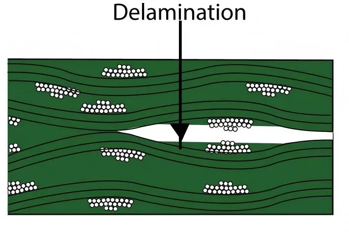
3. Delamination in Thick Copper PCBs
Delamination refers to the separation of layers in a PCB, which can compromise structural integrity and electrical performance. Thick copper PCBs are particularly susceptible due to the mechanical stress from heavy copper and thermal expansion differences.
Causes of Delamination
- Thermal Stress: Repeated heating and cooling cycles during soldering or operation can cause layers to separate.
- Moisture Absorption: Humidity trapped in the board can expand during thermal processes, leading to delamination.
- Poor Adhesion: Inadequate bonding between copper and dielectric materials due to improper lamination or material mismatch.
Troubleshooting Delamination Issues
- Proper Material Selection: Choose laminates with a high glass transition temperature (Tg) above 170°C to withstand thermal stress.
- Bake Before Assembly: Pre-bake boards at 120°C for 2-4 hours to remove moisture before soldering.
- Optimize Lamination Process: Use controlled pressure and temperature during lamination to ensure strong interlayer bonding.
- Minimize Thermal Cycles: Reduce exposure to extreme temperature changes during manufacturing and testing.
Preventing delamination ensures the long-term reliability of thick copper PCBs, especially in harsh environments.
4. Stackup Challenges in Thick Copper PCB Design
The stackup design defines the arrangement of copper and dielectric layers in a PCB. With thick copper, achieving a balanced stackup is critical to prevent warping and ensure signal integrity.
Common Stackup Problems
- Warping: Uneven distribution of copper thickness can cause the board to bend or twist.
- Signal Integrity Issues: Improper layer arrangement can lead to impedance mismatches, affecting high-speed signals.
- Thermal Imbalance: Thick copper layers can create hotspots if not paired with appropriate dielectric materials.
Troubleshooting Stackup Issues
- Balance Copper Distribution: Distribute thick copper layers symmetrically across the stackup to minimize warping. For instance, place 6 oz/ft2 layers on both outer sides of a 4-layer board.
- Calculate Impedance: Use impedance calculators to design trace widths and dielectric thicknesses for controlled impedance, targeting values like 50 ohms for high-speed signals.
- Select Compatible Materials: Pair thick copper with high-Tg or low-CTE (coefficient of thermal expansion) dielectrics to reduce thermal mismatch.
- Simulate Stackup: Use simulation tools to predict thermal and mechanical behavior before fabrication.
A well-designed stackup is the foundation of a reliable thick copper PCB, especially for multilayer boards.
5. Alignment Errors in Thick Copper PCB Production
Alignment, or registration, ensures that layers in a multilayer PCB line up correctly. With thick copper, misalignment can be more pronounced due to the increased layer thickness and manufacturing tolerances.
Common Alignment Problems
- Layer Misregistration: Offset between layers, causing vias or pads to be misaligned.
- Drill Misalignment: Holes not aligning with designed locations, affecting connectivity.
- Signal Integrity Issues: Misalignment can alter trace geometry, impacting high-frequency performance.
Troubleshooting Alignment Issues
- Use Precision Equipment: Employ high-accuracy drilling and imaging systems to maintain tight tolerances, ideally within ±2 mils (0.05 mm).
- Add Registration Marks: Include fiducial marks on each layer for better alignment during lamination and drilling.
- Inspect After Each Step: Perform optical inspections after drilling and lamination to catch misalignment early.
- Control Panel Expansion: Account for material expansion during processing by using stable base materials and controlled temperatures.
Accurate alignment is essential for ensuring connectivity and performance in thick copper multilayer boards.
Best Practices for Thick Copper PCB Manufacturing
Beyond troubleshooting specific issues, adopting best practices can prevent problems from arising in the first place. Here are some key strategies:
- Collaborate Early: Work closely with your fabrication team during the design phase to align on material choices and process capabilities.
- Prototype and Test: Build and test prototypes to identify potential issues before full-scale production.
- Maintain Process Control: Implement strict controls for temperature, pressure, and chemical concentrations during manufacturing.
- Document Issues: Keep detailed records of past problems and solutions to build a knowledge base for future projects.
Conclusion: Mastering Thick Copper PCB Manufacturing
Manufacturing thick copper PCBs comes with unique challenges, but with the right troubleshooting techniques, you can overcome issues related to etching, plating, delamination, stackup, and alignment. By optimizing process parameters, selecting compatible materials, and maintaining precision at every step, you can produce high-quality boards that meet the demands of high-power applications.
At ALLPCB, we're committed to supporting engineers and manufacturers with resources and expertise to tackle these challenges. Whether you're dealing with uneven etching or stackup imbalances, the solutions outlined in this guide can help you achieve reliable, high-performance thick copper PCBs.