ALLPCB


In the world of analog PCB design, grounding is one of the most critical factors for ensuring signal integrity and minimizing noise. Many engineers have long relied on the concept of "star grounding" as a go-to technique for analog PCB grounding. But is it really the best approach? In this comprehensive guide, we debunk the star ground myth and explore effective analog PCB grounding techniques, compare star ground vs ground plane methods, and provide actionable insights for mixed signal PCB grounding and reducing ground loops in analog circuits.
Whether you're designing a high-precision sensor circuit or a mixed-signal board with both analog and digital components, understanding the right grounding strategy can make or break your design. Let’s dive into the details of grounding practices that truly work and why star grounding might not always be the silver bullet it’s often made out to be.
Why Grounding Matters in Analog PCB Design
Grounding in analog PCB design serves as the foundation for stable operation. It provides a reference point for all signals and helps manage noise, electromagnetic interference (EMI), and ground loops. Poor grounding can lead to issues like signal distortion, increased noise levels, and even complete circuit failure. For instance, in a high-gain amplifier circuit, a ground loop could introduce a 60 Hz hum, rendering the output unusable.
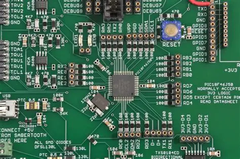
In mixed-signal designs, where analog and digital components coexist, grounding becomes even more complex. Digital circuits often generate high-frequency noise that can interfere with sensitive analog signals. Without proper grounding, a digital clock signal switching at 10 MHz could couple into an analog input, causing errors in measurements or audio distortion.
The goal of effective grounding is to create a low-impedance path for return currents while preventing noise from spreading across the board. This is where techniques like star grounding and ground planes come into play, each with its own strengths and weaknesses.
What Is Star Grounding and Why Is It Popular?
Star grounding is a technique where all ground connections in a circuit are routed to a single central point, resembling the shape of a star. The idea behind this method is to prevent ground loops by ensuring that return currents from different parts of the circuit don’t share a common path, which could lead to voltage differences and noise.
This approach gained popularity in analog designs because it seems intuitive. By connecting all grounds to one point, you theoretically avoid current flowing between different sections of the circuit through the ground. For example, in an audio amplifier board, a star ground might connect the input stage, power supply, and output stage grounds to a single point near the power supply return, aiming to minimize hum and buzz.
However, while star grounding can work in simple, low-frequency circuits, it often falls short in more complex or high-frequency designs. The long traces required to reach the central ground point can act as antennas, picking up or radiating EMI. Additionally, at higher frequencies (above 1 MHz), the impedance of these traces increases, making the star ground less effective as a low-impedance reference.
The Limitations of Star Grounding in Modern Designs
Despite its historical use, star grounding has significant drawbacks that make it less suitable for many modern analog and mixed-signal PCB designs. Let’s break down these limitations:
- Increased Trace Lengths: Routing all ground connections to a single point often results in long traces. These traces have higher inductance, which can cause voltage drops and noise at frequencies as low as 100 kHz. For instance, a 5 cm trace might introduce an inductance of around 50 nH, creating a noticeable impedance at high frequencies.
- EMI Susceptibility: Long ground traces can act as antennas, radiating or picking up electromagnetic interference. This is especially problematic in environments with nearby switching power supplies or RF signals.
- Scalability Issues: In complex designs with dozens or hundreds of components, routing every ground to a single point becomes impractical. It can lead to a cluttered layout and increased board size, driving up manufacturing costs.
- Poor Performance in Mixed-Signal Designs: In boards with both analog and digital components, star grounding fails to address the different noise profiles of each domain. Digital switching currents can still couple into the analog section through the shared ground point, negating the intended isolation.
These issues highlight why star grounding is often more of a myth than a universal solution for analog PCB grounding. While it might work for a simple op-amp circuit on a breadboard, it’s rarely the best choice for production-grade designs.
Ground Planes: A Better Alternative for Analog and Mixed-Signal Designs
Instead of relying on star grounding, many experienced engineers turn to ground planes as a more robust solution for analog PCB grounding techniques. A ground plane is a large, continuous layer of copper on the PCB that serves as a low-impedance ground reference for the entire circuit. Here’s why ground planes often outperform star grounding:
- Low Impedance: A ground plane provides a near-zero impedance path for return currents, even at high frequencies. For example, at 10 MHz, a well-designed ground plane might have an impedance of less than 1 mΩ, compared to several ohms for a long trace in a star ground setup.
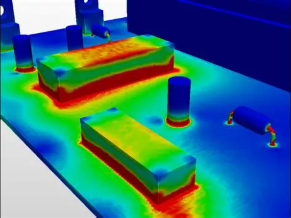
- Reduced EMI: By minimizing the loop area of return currents, a ground plane helps reduce radiated emissions and susceptibility to external interference. This is critical in mixed-signal PCB grounding, where digital noise must be contained.
- Simplified Layout: With a ground plane, there’s no need to route individual ground traces to a single point. Components can connect to the ground plane through short vias, simplifying the design process and reducing board congestion.
- Better for High-Frequency Designs: Ground planes are essential for maintaining signal integrity in high-speed circuits, where return currents need to follow the shortest path under signal traces to avoid impedance mismatches.
In practice, a ground plane can be implemented as a dedicated layer in a multilayer PCB or as a large copper pour on a single-layer board. For mixed-signal designs, splitting the ground plane into analog and digital sections, connected at a single point, often provides the best balance of isolation and low impedance.
Star Ground vs Ground Plane: A Side-by-Side Comparison
To help you choose the right grounding strategy for your design, let’s compare star ground vs ground plane across key metrics:
| Criteria | Star Ground | Ground Plane |
|---|---|---|
| Impedance at High Frequencies | High (due to trace inductance) | Very Low (near-zero impedance) |
| EMI Performance | Poor (long traces act as antennas) | Excellent (minimizes loop area) |
| Suitability for Mixed-Signal | Limited (hard to isolate noise) | Highly Suitable (split planes possible) |
| Ease of Implementation | Complex (requires careful routing) | Simple (dedicated layer or pour) |
From this comparison, it’s clear that ground planes are generally superior for most analog and mixed-signal applications. However, star grounding might still have a niche use in very simple, low-frequency circuits where a ground plane isn’t feasible due to cost or board constraints.
Mixed Signal PCB Grounding: Best Practices for Noise Isolation
In mixed-signal PCB grounding, the challenge is to prevent noisy digital signals from interfering with sensitive analog components. A common approach is to use a split ground plane, where the analog and digital grounds are separated but connected at a single point, often near the power supply or ADC/DAC component.
Here are some best practices for effective mixed-signal grounding:
- Use Split Ground Planes: Designate separate areas of the ground plane for analog and digital circuits. Connect these planes at a single point to avoid ground loops while maintaining a common reference. For example, in a data acquisition system, place the connection point near the ADC to ensure accurate conversion.
- Route Signals Carefully: Keep analog and digital signals on separate layers or areas of the board. Avoid running digital traces over the analog ground plane to prevent capacitive coupling of noise.
- Place Decoupling Capacitors: Use decoupling capacitors (e.g., 0.1 μF ceramic capacitors) close to the power pins of digital ICs to shunt high-frequency noise to ground before it spreads.
- Minimize Return Path Disruptions: Ensure that return currents for high-speed digital signals follow the shortest path under the signal traces. Slots or cuts in the ground plane can force currents to take longer routes, increasing EMI.
By following these guidelines, you can achieve effective noise isolation in mixed-signal designs without resorting to outdated methods like star grounding.
Reducing Ground Loops in Analog Circuits: Practical Tips
Ground loops are a common source of noise in analog circuits, often manifesting as a low-frequency hum or interference. They occur when return currents flow through multiple ground paths, creating small voltage differences that get amplified as noise. Here are actionable tips for reducing ground loops in analog circuits:
- Use a Single Ground Reference: Whether you’re using a ground plane or a carefully designed star point for simple circuits, ensure all components reference the same ground potential. Avoid multiple ground connections that could form loops.
- Keep Power and Ground Close: Route power and ground traces or planes close together to minimize the loop area for return currents. A smaller loop area reduces the chance of picking up external magnetic interference.
- Isolate Sensitive Circuits: For highly sensitive analog circuits, consider using galvanic isolation techniques, such as optocouplers or transformers, to break potential ground loops between different sections of the system.
- Check Cable Connections: Ground loops often arise from external connections, like shielded cables. Ensure that cable shields are grounded at only one end to prevent current flow through the shield.
Implementing these strategies can significantly reduce ground loops, ensuring cleaner signals in your analog designs. For instance, in an audio preamp circuit, grounding the input cable shield at the source end only can eliminate a 60 Hz hum caused by a ground loop.
Conclusion: Moving Beyond the Star Ground Myth
Grounding is a cornerstone of successful analog PCB design, but clinging to outdated methods like star grounding can lead to suboptimal performance, especially in complex or high-frequency circuits. While star grounding may have its place in very simple, low-cost designs, the evidence is clear: ground planes offer superior performance for most modern applications, providing low impedance, reduced EMI, and better scalability.
For mixed-signal PCB grounding, a split ground plane connected at a strategic point often strikes the right balance between noise isolation and simplicity. By adopting these modern analog PCB grounding techniques and focusing on reducing ground loops in analog circuits, you can design boards that deliver reliable, noise-free performance.
At ALLPCB, we’re committed to helping engineers achieve the best possible results in their PCB designs. By understanding the limitations of star grounding and embracing more effective alternatives like ground planes, you’ll be well on your way to creating high-quality analog and mixed-signal circuits that stand the test of time.