 ALLPCB


Designing with thick copper PCBs is a game-changer for high-power applications, but it comes with unique challenges. If you're wondering how to optimize your design for thick copper PCB design rules, high current trace width, via design, or solder mask considerations, you're in the right place. This guide from ALLPCB offers actionable PCB design guidelines to help you navigate these complexities and create reliable, efficient boards for demanding projects.
In this comprehensive blog, we'll dive deep into the essentials of working with thick copper PCBs. From understanding why thick copper is crucial for high-current applications to practical tips on trace width calculations and via design, we've got you covered. Let's explore how to elevate your PCB designs with precision and confidence.
Why Choose Thick Copper PCBs for Your Design?
Thick copper PCBs are specialized circuit boards with copper layers significantly thicker than standard boards, often ranging from 3 oz/ft2 (105 μm) to 20 oz/ft2 (700 μm) or more. These boards are ideal for applications requiring high current carrying capacity, such as power electronics, automotive systems, and industrial equipment. The increased copper thickness reduces resistance, improves heat dissipation, and enhances overall durability.
Using thick copper in your PCB design offers several benefits:
- Higher Current Capacity: Thicker copper traces can handle currents exceeding 10A without overheating.
- Better Thermal Management: Thick copper dissipates heat more effectively, preventing hotspots that can damage components.
- Enhanced Mechanical Strength: The added copper thickness makes the board more robust, ideal for harsh environments.
However, designing with thick copper requires careful planning to avoid issues like uneven etching, increased manufacturing costs, or signal integrity problems. Let's break down the key PCB design guidelines to ensure success.
Thick Copper PCB Design Rules: Key Considerations
When designing with thick copper, following specific design rules is critical to ensure manufacturability and performance. Here are the fundamental thick copper PCB design rules to keep in mind:
1. Understand Copper Thickness and Manufacturing Limits
The copper thickness you choose impacts both performance and manufacturing feasibility. For instance, a 6 oz/ft2 (210 μm) copper layer can carry significantly more current than a 1 oz/ft2 (35 μm) layer, but it may require specialized etching processes. Most manufacturers can handle up to 6 oz/ft2 with standard processes, while thicker layers (10 oz/ft2 or more) often need custom fabrication techniques, increasing lead time and cost.
Tip: Consult with your PCB manufacturer early in the design phase to confirm their capabilities for thick copper layers. Specify whether the thickness is for inner layers, outer layers, or both.
2. Account for Increased Board Weight and Thickness
Thick copper adds weight and bulk to your PCB. A board with 10 oz/ft2 copper on both sides can be noticeably heavier, affecting mounting and mechanical design. Additionally, the overall board thickness may increase, impacting enclosure designs or connector compatibility.
Tip: Factor in the final board dimensions and weight during the initial design to avoid surprises during assembly.
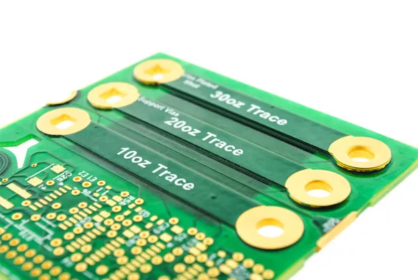
High Current Trace Width: Sizing for Safety and Efficiency
One of the most critical aspects of designing with thick copper PCBs is determining the appropriate trace width for high current applications. Undersized traces can overheat, leading to performance issues or even board failure. Here's how to calculate and optimize high current trace width effectively.
Calculating Trace Width for High Current
The width of a trace must be sufficient to handle the expected current without exceeding a safe temperature rise. A common guideline is to use a temperature rise of 10°C to 20°C above ambient as a safe limit. The required trace width depends on the copper thickness, current, and ambient conditions.
For example, according to industry-standard charts like those based on IPC-2221, a 1 oz/ft2 copper trace carrying 5A requires a width of approximately 0.2 inches (5 mm) for a 10°C temperature rise. However, with a 6 oz/ft2 thick copper layer, the same 5A current needs only about 0.03 inches (0.76 mm) of width due to the increased cross-sectional area.
Tip: Use online trace width calculators or refer to IPC standards for precise calculations. Always add a safety margin (e.g., 20-30% wider traces) to account for manufacturing variations or unexpected current spikes.
Balancing Trace Width with Board Space
While wider traces are better for high current, they consume more board space, which can be a constraint in compact designs. Thick copper allows narrower traces for the same current, freeing up space for other components or routing.
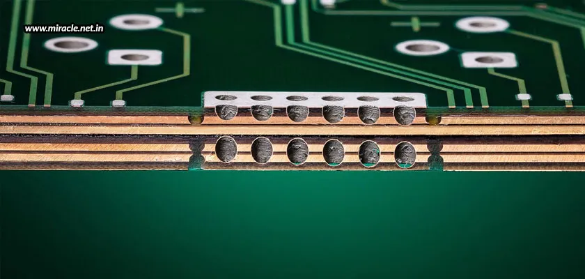
Via Design for Thick Copper PCBs: Ensuring Reliability
Vias play a crucial role in thick copper PCB designs, especially for high-current applications where they must carry significant current between layers. Poor via design can lead to overheating, cracking, or insufficient current capacity. Let's explore the best practices for via design in thick copper PCBs.
Choosing the Right Via Size and Type
In high-current designs, vias must have enough copper plating to handle the load. Standard vias with 1 mil (25 μm) of copper plating may suffice for signal traces but are inadequate for power traces. For thick copper PCBs, use vias with heavier plating (e.g., 2-3 mil or 50-75 μm) or opt for filled vias to increase current capacity and thermal conductivity.
For example, a via with a 0.01-inch (0.25 mm) diameter and 2 mil copper plating can carry approximately 1-2A safely. For higher currents, increase the via diameter or use multiple vias in parallel to distribute the load.
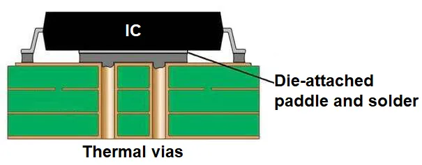
Thermal Vias for Heat Dissipation
In thick copper designs, thermal vias are often used to transfer heat from components to a copper plane or heatsink. Place an array of vias under high-power components like MOSFETs to enhance cooling. Ensure the vias are connected to a large copper area for maximum heat dissipation.
Tip: Avoid overfilling vias with solder during assembly, as this can create voids or reduce thermal performance. Specify via filling or capping if needed.
Solder Mask Considerations for Thick Copper PCBs
The solder mask is a protective layer on a PCB that prevents short circuits and oxidation. However, with thick copper PCBs, applying solder mask requires special attention due to the increased copper height and potential for uneven surfaces.
Adjusting Solder Mask Thickness
Standard solder mask thickness (typically 0.5-1 mil or 12-25 μm) may not fully cover thick copper traces, especially at edges where copper height is pronounced (e.g., 6 oz/ft2 or higher). This can lead to exposed copper, increasing the risk of corrosion or shorts. Request a thicker solder mask layer (e.g., 1.5-2 mil or 38-50 μm) to ensure complete coverage.
Defining Solder Mask Clearances
Thick copper traces often have sharper edges due to the etching process, which can cause solder mask adhesion issues. Increase the solder mask clearance around pads and traces to prevent cracking or peeling. A clearance of 4-6 mil (0.1-0.15 mm) beyond the copper edge is often recommended for thick copper designs.
Tip: Specify solder mask requirements clearly in your design files to avoid manufacturing defects. Consider using a liquid photoimageable (LPI) solder mask for better coverage on uneven surfaces.
Additional PCB Design Guidelines for Thick Copper
Beyond trace width, via design, and solder mask, here are additional PCB design guidelines to optimize your thick copper PCB:
1. Optimize Copper Balancing
Thick copper layers can cause uneven stress during manufacturing, leading to board warpage. Balance copper distribution across layers by adding dummy copper fills or mirroring copper areas on opposite sides of the board. This helps maintain flatness and prevents mechanical issues.
2. Plan for Etching Challenges
Thick copper requires longer etching times, which can result in undercutting or uneven trace edges. Work with your manufacturer to adjust trace spacing and avoid fine-pitch designs (below 6 mil or 0.15 mm) on thick copper layers unless absolutely necessary.
3. Consider Cost Implications
Thick copper PCBs are more expensive due to additional material and specialized processes. Optimize your design by using thick copper only where high current is required, and standard copper (e.g., 1-2 oz/ft2) for signal traces to keep costs down.
Applications of Thick Copper PCBs
Thick copper PCBs are indispensable in industries where power and reliability are paramount. Common applications include:
- Power Supplies: High-current traces and vias support efficient power delivery in AC-DC converters or inverters.
- Automotive Electronics: Thick copper handles the high currents and thermal loads in electric vehicle battery management systems.
- Industrial Controls: Robust designs withstand harsh conditions in motor drives and welding equipment.
By following the guidelines above, you can tailor your thick copper PCB design to meet the specific demands of these applications.
Conclusion: Mastering Thick Copper PCB Design
Designing with thick copper PCBs opens up new possibilities for high-power and high-reliability applications, but it demands careful attention to detail. By adhering to thick copper PCB design rules, optimizing high current trace width, refining via design, and addressing solder mask challenges, you can create boards that perform exceptionally well under demanding conditions.
At ALLPCB, we're committed to supporting your design journey with expert manufacturing services and resources. Whether you're working on a power supply, automotive system, or industrial project, use these PCB design guidelines to ensure your thick copper PCB meets both performance and manufacturability standards. Start optimizing your designs today for unmatched efficiency and durability.


