 ALLPCB


In the world of renewable energy, solar power systems are at the forefront, and the efficiency of these systems often depends on the design of their printed circuit boards (PCBs). If you're looking to create a high-efficiency solar PCB, the key lies in balancing power delivery with effective thermal management. This blog will guide you through the essential techniques for designing solar PCBs that maximize performance while minimizing power loss and heat buildup. We'll dive into topics like solar PCB thermal vias, MPPT controller PCB layout, heat dissipation techniques for solar PCBs, and strategies for minimizing power loss in solar PCB designs.
Whether you're an engineer working on solar inverters, charge controllers, or energy storage systems, this comprehensive guide will provide actionable insights to optimize your designs. Let's explore how to achieve high efficiency in solar PCB design while tackling the challenges of heat and power management.
Why High-Efficiency Solar PCB Design Matters
Solar power systems convert sunlight into usable electricity, but inefficiencies in the PCB design can lead to energy losses and overheating, reducing the overall performance of the system. A high-efficiency solar PCB design ensures that power is delivered with minimal loss while keeping components cool to extend their lifespan. Poorly designed PCBs can result in up to 20% energy loss due to resistance and heat generation, which directly impacts the return on investment for solar installations.
Efficient designs also play a critical role in supporting advanced features like Maximum Power Point Tracking (MPPT) controllers, which optimize energy harvest from solar panels. By focusing on both power delivery and thermal management, you can create reliable, long-lasting solar systems that perform at their peak.
Key Principles of High-Efficiency Solar PCB Design
Designing a solar PCB for maximum efficiency requires attention to several core principles. These include optimizing power flow, reducing resistance, and ensuring proper heat dissipation. Below are the fundamental aspects to consider for achieving high performance.
1. Optimize Component Placement for Power Efficiency
The layout of components on a solar PCB directly affects its efficiency. Place high-power components, such as MOSFETs and diodes in MPPT controllers, close to their corresponding power paths to minimize trace lengths. Longer traces increase resistance, which can lead to power losses of up to 5-10% in high-current applications. For example, a 0.1-ohm increase in trace resistance in a 10A circuit can cause a 1W power loss per trace, which adds up quickly in complex designs.
Additionally, group components that generate heat together and position them away from heat-sensitive parts like microcontrollers. This reduces the risk of thermal interference and helps maintain stable operation.
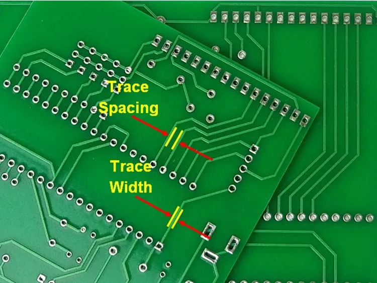
2. Use Wider Traces for High-Current Paths
Solar PCBs often handle high currents, especially in systems with large solar arrays. Narrow traces can create bottlenecks, increasing resistance and leading to voltage drops. Use trace width calculators to determine the appropriate width based on current and copper thickness. For instance, a 10A current on a 1oz copper PCB typically requires a trace width of at least 2.5mm to avoid excessive heating and power loss.
Wider traces not only reduce resistance but also help dissipate heat more effectively, contributing to the overall thermal management of the board.
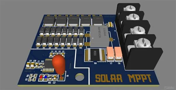
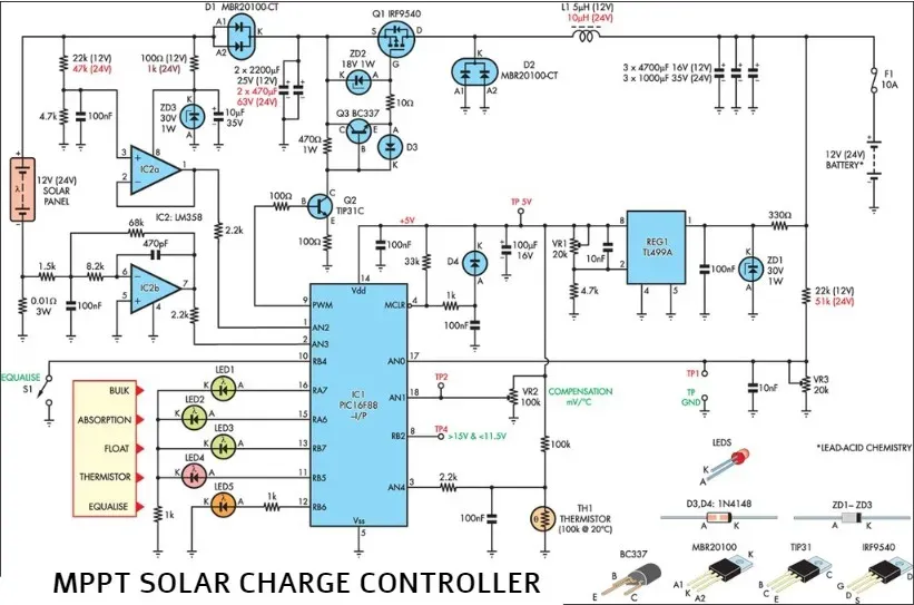
Mastering MPPT Controller PCB Layout for Solar Systems
Maximum Power Point Tracking (MPPT) controllers are the heart of many solar systems, ensuring that panels operate at their optimal voltage and current for maximum energy harvest. A well-designed MPPT controller PCB layout is critical for high efficiency and reliability.
1. Minimize Loop Areas in Switching Circuits
MPPT controllers rely on high-frequency switching to regulate power, which can generate electromagnetic interference (EMI) if not handled properly. Keep the switching loop areas small by placing inductors, capacitors, and MOSFETs as close together as possible. A smaller loop reduces inductance and minimizes noise, which can improve efficiency by up to 2-3% in high-frequency designs operating at 100kHz or above.
2. Separate Analog and Digital Grounds
MPPT controllers often include both analog and digital circuitry. Mixing their ground planes can introduce noise into sensitive analog signals, affecting accuracy. Use separate ground planes connected at a single point (star grounding) to isolate noise and ensure clean power delivery. This technique is especially important in designs where the MPPT controller interfaces with microcontrollers for data logging or remote monitoring.
Effective Heat Dissipation Techniques for Solar PCBs
Thermal management is a major challenge in solar PCB design due to the high power levels and outdoor operating conditions. Excessive heat can degrade components, reduce efficiency, and shorten the lifespan of the system. Let's explore proven heat dissipation techniques for solar PCBs to keep temperatures under control.
1. Incorporate Solar PCB Thermal Vias
Thermal vias are small holes filled or plated with copper that transfer heat from one layer of the PCB to another, often to a heat sink or copper plane. In solar PCBs, place thermal vias under high-power components like power transistors or regulators to channel heat away from the surface. For example, a grid of 0.3mm vias with 1.2mm spacing can reduce the temperature of a component by 10-15°C, depending on the design and airflow.
Ensure that vias are connected to large copper areas on the opposite side of the board to maximize heat spreading. However, avoid placing vias directly under solder pads if they might interfere with soldering processes.
2. Use Heat Sinks for High-Power Components
Heat sinks are passive cooling devices that increase the surface area for heat dissipation. Attach heat sinks to components that generate significant heat, such as voltage regulators or power diodes. Choose materials like aluminum or copper for their high thermal conductivity (around 200-400 W/m·K). For instance, a small aluminum heat sink can lower the operating temperature of a component by 20°C or more, depending on ambient conditions and airflow.
In outdoor solar applications, ensure that heat sinks are designed to withstand environmental factors like dust and moisture by using protective coatings or enclosures.
3. Leverage Copper Planes for Heat Spreading
Large copper planes on the PCB act as natural heat spreaders, distributing thermal energy across a wider area. Dedicate entire layers or large sections of the board to copper pours connected to ground or power planes. This technique can reduce localized hot spots by 5-10°C, especially in multilayer boards where heat can be transferred vertically through vias.
Strategies for Minimizing Power Loss in Solar PCBs
Power loss in solar PCBs not only reduces efficiency but also contributes to heat generation, creating a vicious cycle. Minimizing power loss in solar PCB designs is essential for high performance. Here are actionable strategies to achieve this goal.
1. Select Low-Resistance Components
Choose components with low on-resistance (RDS(on)) for MOSFETs and low forward voltage drops for diodes. For example, using a MOSFET with an RDS(on) of 10mΩ instead of 50mΩ in a 10A circuit can reduce power loss from 5W to 1W per component. These savings add up in systems with multiple switching elements, directly boosting efficiency.
2. Optimize PCB Layer Stackup
In multilayer solar PCBs, the stackup design affects both power delivery and heat management. Place power and ground planes adjacent to each other to reduce loop inductance and improve current flow. A typical 4-layer stackup for a solar PCB might include a top signal layer, an inner power plane, an inner ground plane, and a bottom signal layer. This configuration minimizes impedance and can reduce power losses by up to 3-5% in high-current designs.
3. Reduce Parasitic Effects
Parasitic capacitance and inductance in PCB traces can cause switching losses in high-frequency circuits like MPPT controllers. Keep traces short and direct, and avoid sharp corners that can act as antennas for EMI. Use rounded corners or 45-degree angles for trace routing to minimize these effects. Reducing parasitic losses can improve efficiency by 1-2%, which is significant in large solar arrays.
Balancing Power and Thermal Management: A Holistic Approach
High-efficiency solar PCB design is not just about optimizing power or managing heat in isolation—it's about finding the right balance between the two. A design that prioritizes power delivery but neglects thermal management will overheat, while a design focused solely on cooling might compromise efficiency with overly conservative component choices.
Start by simulating your design using thermal and power analysis tools to predict hot spots and efficiency losses. Adjust component placement, trace widths, and cooling solutions based on the simulation results. For instance, if a simulation shows a 30°C temperature rise near a power regulator, consider adding thermal vias or a small heat sink to bring it down to a safe level (typically below 85°C for most components).
Iterate on your design by testing prototypes under real-world conditions, such as full sunlight exposure or high ambient temperatures. Outdoor solar systems often operate in temperatures ranging from -20°C to 50°C, so ensure your PCB can handle these extremes without efficiency drops or thermal failures.
Conclusion: Building the Future of Solar Power with Efficient PCB Design
Designing high-efficiency solar PCBs is a complex but rewarding endeavor. By focusing on key areas like MPPT controller PCB layout, solar PCB thermal vias, heat dissipation techniques, and minimizing power loss, you can create systems that deliver maximum energy output while maintaining reliability. These strategies not only improve performance but also contribute to the sustainability of solar power by reducing waste and extending system lifespan.
Whether you're working on small residential solar setups or large commercial arrays, the principles of balancing power and thermal management remain the same. Apply the techniques discussed in this guide to elevate your solar PCB designs and stay ahead in the rapidly evolving field of renewable energy.


