ALLPCB


In the fast-evolving world of electronics, the demand for smaller, lighter, and more powerful devices continues to grow. This is where High-Density Interconnects (HDI) on thin PCBs come into play. If you're wondering how to design an HDI thin PCB for optimal performance, the answer lies in leveraging advanced techniques like microvias, via-in-pad layouts, and careful signal integrity management. These methods allow you to pack more functionality into a smaller space while maintaining reliability and performance. In this blog, we'll dive deep into the world of HDI thin PCB design, exploring key concepts, practical tips, and best practices to help you master high-density thin PCB layouts.
What Are High-Density Interconnects (HDI) on Thin PCBs?
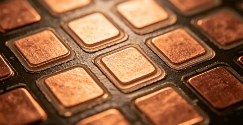
High-Density Interconnects, or HDI, refer to a PCB design approach that uses finer lines, smaller vias, and denser component placement to achieve higher functionality in a limited space. When applied to thin PCBs—boards with reduced thickness often below 0.8 mm—HDI technology becomes even more critical. These thin boards are essential for compact devices like smartphones, wearables, and medical equipment, where every millimeter counts.
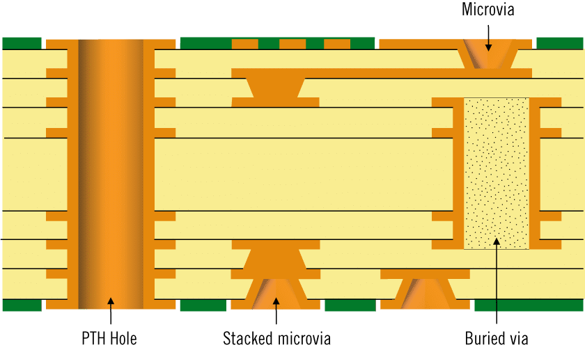
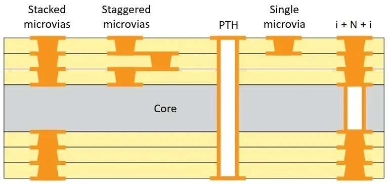
An HDI thin PCB typically incorporates microvias (vias with diameters less than 0.15 mm), blind and buried vias, and advanced layout strategies like via-in-pad. These elements reduce the board's footprint while maintaining or even improving electrical performance. The result is a lightweight, compact board that can handle complex circuits without sacrificing signal integrity.
Why Choose HDI for Thin PCB Designs?
The benefits of using HDI on thin PCBs are numerous, especially for industries pushing the boundaries of miniaturization. Here are some key reasons why this approach is a game-changer:
- Space Efficiency: HDI allows for tighter component placement, reducing the overall size of the board. This is critical for thin PCBs used in ultra-compact devices.
- Improved Signal Integrity: By using shorter signal paths and techniques like via-in-pad, HDI minimizes signal loss and interference, ensuring reliable performance even at high frequencies (e.g., above 1 GHz).
- Reduced Weight: Thin PCBs with HDI are lighter, making them ideal for portable and wearable electronics.
- Enhanced Reliability: Microvias in HDI designs have a smaller aspect ratio (typically below 1:1), which improves durability compared to traditional through-hole vias under thermal stress.
With these advantages, it's clear why HDI thin PCB design is becoming the go-to choice for modern electronics. However, achieving these benefits requires careful planning and precise execution.
Key Techniques for HDI Thin PCB Design
Designing an HDI thin PCB is not just about shrinking components or reducing board thickness. It involves mastering specific techniques to ensure functionality and reliability. Let's explore the critical elements of this process, focusing on microvia thin PCB structures, via-in-pad layouts, and high-density thin PCB layout strategies.
1. Leveraging Microvias in Thin PCB Designs
Microvias are tiny vias, often created using laser drilling, with diameters typically ranging from 0.05 mm to 0.15 mm. In a microvia thin PCB, these small vias connect adjacent layers without penetrating the entire board, saving space and enabling denser routing.
Unlike traditional through-hole vias, microvias offer several benefits:
- They allow for finer pitch components, such as 0.4 mm pitch Ball Grid Arrays (BGAs).
- They reduce parasitic capacitance and inductance, improving signal integrity on thin PCBs.
- They support blind and buried via configurations, freeing up space on outer layers for additional components.
However, microvias come with challenges. Their small size makes them prone to thermal stress during assembly, which can lead to cracking if not designed properly. To mitigate this, ensure the aspect ratio (via depth to diameter) stays below 1:1, and use high-quality materials with low coefficients of thermal expansion (CTE), such as polyimide-based laminates.
2. Implementing Via-in-Pad for High-Density Layouts
Via-in-pad is a technique where vias are placed directly under component pads, rather than routing them to separate areas on the board. This method is especially useful in a via-in-pad thin PCB design, as it maximizes space efficiency and supports high-density layouts.
The primary advantage of via-in-pad is the reduction of signal path length. For high-speed signals, shorter paths mean less signal delay and better performance. For example, in a design with a 5 GHz signal, reducing the trace length by even 1 mm can lower latency and improve signal integrity.
To implement via-in-pad effectively, consider these tips:
- Use microvias for via-in-pad to minimize the pad size and avoid solder wicking during assembly.
- Ensure the via is filled and capped with a conductive material to create a flat surface for component mounting.
- Work with your fabrication partner to confirm their capabilities for via-in-pad processes, as this technique requires precise manufacturing.
While via-in-pad boosts density, it can increase manufacturing costs due to the additional steps involved. Balance the benefits against your project budget to decide if this approach fits your needs.
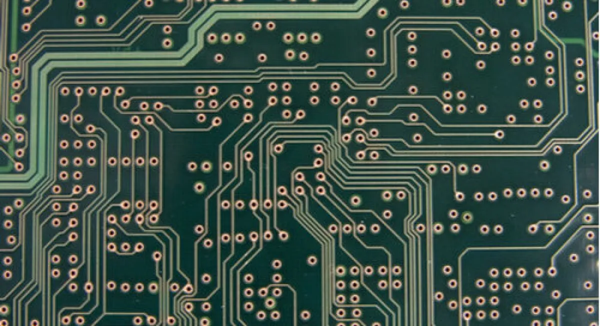
3. Optimizing High-Density Thin PCB Layouts
A high-density thin PCB layout requires careful planning to fit more components and traces into a limited area without compromising performance. Here are some strategies to achieve an effective layout:
- Fine Line Widths and Spacing: Use trace widths as small as 0.075 mm (3 mils) and spacing down to 0.075 mm to increase routing density. This allows more traces between component pins, especially for fine-pitch devices.
- Stackup Design: Opt for a multilayer stackup with 6 or more layers in an HDI thin PCB. Alternate signal and ground layers to create a controlled impedance environment (e.g., 50 ohms for high-speed signals).
- Component Placement: Group related components closely to minimize trace lengths, and place high-speed components near connectors to reduce signal travel distance.
By focusing on these layout techniques, you can achieve a compact yet functional design that meets the demands of modern electronics.
Ensuring Signal Integrity in Thin PCB Designs
Signal integrity is a critical concern in any PCB design, but it becomes even more challenging with an HDI thin PCB. Thin boards have limited space for ground planes and shielding, and high-density layouts increase the risk of crosstalk and electromagnetic interference (EMI). Here's how to maintain signal integrity in thin PCB designs:
1. Minimize Crosstalk with Proper Layering
Crosstalk occurs when signals on adjacent traces interfere with each other, degrading performance. To prevent this, use ground planes between signal layers in your stackup. For instance, a 6-layer HDI thin PCB could follow a signal-ground-signal-power-ground-signal configuration to isolate high-speed traces.
2. Control Impedance for High-Speed Signals
High-speed signals, such as those operating at 2.5 Gbps or higher, require controlled impedance to prevent reflections. Calculate the trace width and dielectric thickness to achieve the target impedance, typically 50 ohms for single-ended signals or 100 ohms for differential pairs. Use simulation tools to verify impedance before fabrication.
3. Avoid Split Planes and Long Traces
Ensure that high-speed signals do not cross split planes in the ground or power layers, as this disrupts the return path and causes EMI. Keep trace lengths short to reduce signal delay—for example, a 10 mm trace at 3 GHz introduces a delay of approximately 50 ps, which can impact timing in critical designs.
By prioritizing signal integrity in thin PCB designs, you can ensure reliable operation even in the most demanding applications.
Challenges and Solutions in HDI Thin PCB Design
While HDI thin PCBs offer incredible benefits, they come with unique challenges. Understanding these obstacles and how to overcome them is key to a successful design.
- Thermal Management: Thin PCBs have less material to dissipate heat, which can lead to overheating in high-density designs. Use thermal vias and heat sinks to manage temperature, and select materials with high thermal conductivity.
- Manufacturing Complexity: Techniques like microvias and via-in-pad require advanced fabrication processes, increasing costs. Partner with a reliable manufacturer who specializes in HDI to ensure quality.
- Design Complexity: High-density layouts are harder to route and test. Use design software with HDI-specific features to automate routing and validate signal integrity.
Addressing these challenges upfront will save time and resources in the long run, ensuring your HDI thin PCB performs as intended.
Best Practices for HDI Thin PCB Fabrication
Fabrication plays a crucial role in the success of an HDI thin PCB. Here are some best practices to follow when preparing your design for manufacturing:
- Adhere to design rules for microvia aspect ratios (e.g., 0.8:1 or lower) to ensure reliability.
- Specify material requirements, such as high-Tg FR-4 or polyimide, to withstand thermal stress during assembly.
- Include detailed notes on via filling and capping for via-in-pad designs to avoid assembly issues.
- Collaborate closely with your fabrication team to confirm capabilities for fine line widths (e.g., below 0.1 mm) and tight tolerances.
By aligning your design with manufacturing capabilities, you can avoid costly revisions and delays.
Conclusion: Mastering HDI Thin PCB Design
Designing for density with High-Density Interconnects on thin PCBs is a powerful way to meet the demands of modern electronics. By leveraging techniques like microvia thin PCB structures, via-in-pad layouts, and optimized high-density thin PCB layouts, you can create compact, reliable, and high-performing boards. Prioritizing signal integrity in thin PCB designs ensures that even the most complex circuits operate flawlessly.
Whether you're working on a wearable device, a medical implant, or a cutting-edge mobile gadget, mastering HDI thin PCB design opens up new possibilities for innovation. With careful planning, attention to detail, and collaboration with experienced fabrication partners, you can bring your high-density designs to life with confidence.