 ALLPCB


If you're looking to understand the buried via PCB manufacturing process, you're in the right place. Buried vias are essential for creating high-density interconnects in modern printed circuit boards (PCBs), allowing connections between internal layers without reaching the outer surfaces. This guide will walk you through every step of buried via fabrication, from design considerations to drilling techniques, plating processes, inspection methods, and sequential lamination for buried vias. Whether you're a PCB designer or manufacturer, this detailed resource will help you master the process with practical insights and actionable steps.
What Are Buried Vias and Why Do They Matter?
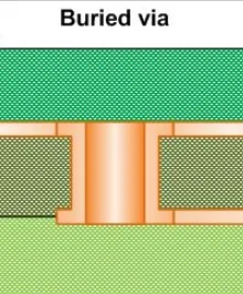
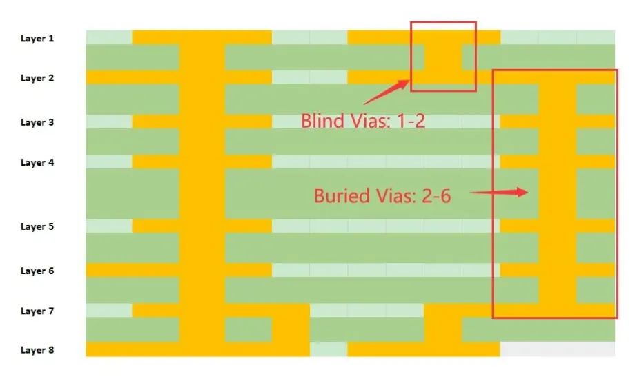
Buried vias are specialized connections that link two or more internal layers of a PCB without extending to the board's outer surfaces. Unlike through-hole vias, which pass through the entire board, or blind vias, which connect an outer layer to an inner one, buried vias remain hidden inside the board. This unique structure makes them ideal for high-density designs where space is limited, and signal integrity is critical.
In modern electronics, buried vias play a vital role in reducing board size while maintaining performance. They allow for more compact layouts, minimize signal interference, and improve routing efficiency. For example, in multilayer boards used in smartphones or aerospace applications, buried vias can help achieve layer counts of 12 or more while keeping the board thickness under 1.6 mm. Their ability to hide connections within internal layers also enhances the overall aesthetics and functionality of the PCB.
Step 1: Design Considerations for Buried Via PCB Manufacturing Process
Before diving into fabrication, proper design is the foundation of successful buried via integration. During the design phase, manufacturers and engineers must consider several factors to ensure the vias function as intended and the board remains reliable.
- Layer Stack-Up Planning: Determine the placement of buried vias within the internal layers. For instance, a 10-layer board might have buried vias connecting layers 3 to 5 and 6 to 8. This requires precise stack-up planning to avoid interference with other components or traces.
- Aspect Ratio: The aspect ratio (via depth to diameter) for buried vias should typically be kept below 10:1 to ensure manufacturability. A via with a diameter of 0.2 mm should not exceed a depth of 2 mm to avoid drilling and plating issues.
- Signal Integrity: Buried vias help reduce signal loss in high-speed designs. For applications requiring frequencies above 5 GHz, shorter buried vias can minimize impedance mismatches, often keeping impedance variations below 5%.
- Thermal Management: Ensure buried vias are not placed in areas prone to excessive heat, as they can act as thermal conduits, potentially causing delamination if temperatures exceed 150°C during operation.
Using advanced PCB design software with simulation tools can help predict potential issues before manufacturing begins. This step sets the stage for a smooth buried via PCB manufacturing process.
Step 2: Buried Via Drilling Techniques
Drilling is a critical step in the buried via fabrication process, as these vias are created before the full board is laminated together. Unlike through-hole vias, buried vias cannot be drilled after the board is fully assembled, making precision essential.
Key Drilling Techniques:
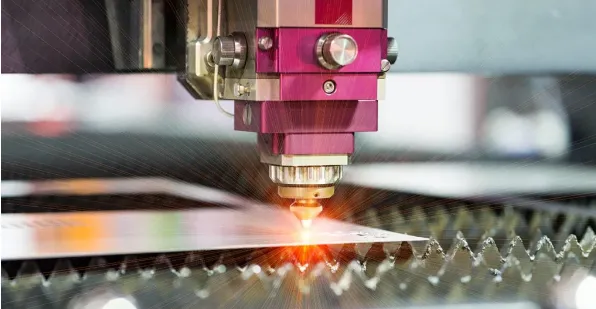
- Laser Drilling: For small-diameter buried vias (often less than 0.15 mm), laser drilling is the preferred method. It offers high precision and minimal thermal damage, creating clean holes with smooth walls. This technique is ideal for high-density interconnect (HDI) boards where microvias are common.
- Mechanical Drilling: For larger buried vias (0.2 mm and above), mechanical drilling with CNC machines is used. However, this method requires careful control to avoid burrs, which can affect plating quality. Spindle speeds often range from 80,000 to 120,000 RPM to achieve clean cuts.
- Depth Control: Since buried vias only span specific internal layers, depth-controlled drilling is crucial. Modern equipment can achieve depth accuracy within ±0.025 mm, ensuring the via stops at the correct layer without damaging adjacent ones.
After drilling, a deburring process removes any rough edges or debris from the holes. Smooth walls are necessary for the next step—plating—to ensure reliable electrical connections.
Step 3: Buried Via Plating Process
Once the holes for buried vias are drilled, they must be plated with a conductive material, typically copper, to establish electrical connections between layers. The buried via plating process is more complex than plating through-hole vias because the vias are inaccessible after final lamination.
Key Steps in Plating:
- Cleaning: The drilled holes are cleaned using a chemical solution to remove debris and oxides. This ensures the copper adheres properly to the via walls.
- Electroless Copper Deposition: A thin layer of copper (about 0.5 to 1 μm) is deposited on the via walls through an electroless process. This creates a conductive base for further plating.
- Electroplating: Additional copper is added via electroplating to achieve a thickness of 20 to 25 μm, ensuring durability and conductivity. Uniform plating is critical to avoid voids or weak spots, which can lead to signal loss or failure under thermal stress.
- Quality Check: Post-plating, the vias are inspected for uniform thickness and adhesion. Poor plating can result in open circuits or increased resistance, often exceeding 10 mΩ per via, which is unacceptable for high-speed designs.
The plating process must be carefully controlled, especially since buried vias cannot be reworked once the board is fully laminated. Precision here directly impacts the board's reliability.
Step 4: Sequential Lamination for Buried Vias
Sequential lamination is a cornerstone of buried via fabrication, as it allows manufacturers to build multilayer PCBs layer by layer, incorporating buried vias at specific stages. This process differs from standard lamination, where all layers are bonded simultaneously.
How Sequential Lamination Works:
- Initial Layer Bonding: The internal layers that will contain buried vias are laminated first. For example, in a 12-layer board, layers 3 to 6 might be bonded together after drilling and plating the buried vias between them.
- Via Formation: Buried vias are drilled and plated in these sub-assemblies before additional layers are added. This ensures the vias remain hidden within the internal structure.
- Additional Lamination Cycles: Subsequent layers are added through additional lamination cycles, often under controlled heat (around 180°C) and pressure (up to 300 psi) to prevent misalignment or delamination.
- Alignment Precision: Misalignment during sequential lamination can cause buried vias to shift, leading to connectivity issues. Modern alignment systems achieve accuracy within ±0.05 mm to prevent such errors.
Sequential lamination for buried vias increases manufacturing complexity and cost but is necessary for HDI designs. It allows for layer counts exceeding 20 while maintaining board thicknesses as low as 1 mm.
Step 5: Buried Via Inspection Methods
Inspection is a critical final step in the buried via PCB manufacturing process. Since buried vias are hidden within the board, detecting defects requires specialized techniques to ensure quality and reliability.
Common Inspection Methods:
- X-Ray Inspection: X-ray imaging is used to examine the internal structure of the PCB, revealing misaligned or poorly plated buried vias. This non-destructive method can detect voids or cracks with a resolution of 0.01 mm.
- Microsectioning: A small sample of the board is cut and polished to expose the buried vias for microscopic analysis. This destructive method checks plating thickness and via integrity, ensuring copper thickness meets the target of 20 μm or more.
- Electrical Testing: Continuity tests verify that buried vias provide proper electrical connections between layers. Resistance values are measured, with acceptable limits often below 5 mΩ per via for high-performance boards.
- Thermal Imaging: During stress testing, thermal cameras detect hotspots around buried vias, indicating potential plating or lamination issues if temperatures rise above 120°C under load.
These buried via inspection methods ensure that the final product meets industry standards, such as IPC-6012 for rigid PCBs, and performs reliably in real-world applications.
Challenges in Buried Via Fabrication and How to Overcome Them
While buried vias offer significant advantages, their fabrication comes with unique challenges. Understanding these obstacles and their solutions can help manufacturers achieve better results.
- Drilling Precision: Inaccurate drilling can damage adjacent layers. Using advanced laser drilling systems with automated depth control minimizes this risk.
- Plating Uniformity: Uneven copper plating can cause reliability issues. Implementing strict process controls and regular equipment calibration ensures consistent results.
- Lamination Misalignment: During sequential lamination, layers can shift, misaligning buried vias. High-precision alignment tools and fiducial markers on each layer help maintain accuracy.
- Cost and Time: The buried via PCB manufacturing process is more expensive and time-consuming than standard through-hole methods. Optimizing designs to minimize via counts and planning efficient lamination cycles can reduce costs.
By addressing these challenges, manufacturers can produce high-quality PCBs with buried vias that meet the demands of modern electronics.
Benefits of Buried Vias in Modern PCB Designs
Buried vias are a game-changer for high-density PCB designs. Their key benefits include:
- Space Savings: By eliminating surface connections, buried vias free up space for additional components, reducing board size by up to 30% in some designs.
- Improved Signal Integrity: Shorter via lengths reduce signal delay and crosstalk, supporting high-speed signals above 10 Gbps with minimal loss.
- Enhanced Reliability: Hidden vias are less exposed to environmental factors like moisture or dust, improving long-term durability in harsh conditions.
These advantages make buried vias indispensable for applications like 5G technology, automotive electronics, and medical devices.
Conclusion: Mastering Buried Via Fabrication
Buried via fabrication is a complex but rewarding process in modern PCB manufacturing. From precise buried via drilling techniques to the intricate buried via plating process, each step requires attention to detail and advanced technology. Sequential lamination for buried vias ensures these connections are seamlessly integrated into multilayer boards, while thorough buried via inspection methods guarantee quality and performance.
By following this step-by-step guide, manufacturers can navigate the challenges of the buried via PCB manufacturing process and produce high-quality boards that meet the demands of cutting-edge electronics. With buried vias, you can achieve greater design flexibility, improved signal integrity, and compact layouts that push the boundaries of innovation.


