 ALLPCB


In the fast-evolving world of telecommunications, the demand for compact, high-performance printed circuit boards (PCBs) is higher than ever. Base stations, which form the backbone of wireless communication networks, require PCBs that can handle complex signals and high-density layouts. This is where blind via PCB and buried via PCB technologies come into play. These advanced via types, often used in HDI PCB designs, significantly enhance telecommunication PCB density and improve performance. In this blog, we’ll dive deep into how blind and buried vias work, their benefits for base station PCBs, and why they are essential for modern telecommunication systems.
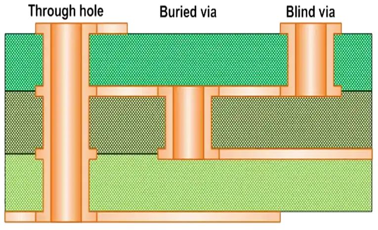
What Are Blind and Buried Vias in PCBs?
Vias are small holes in a PCB that connect different layers, allowing electrical signals to pass through. While traditional through-hole vias go all the way through the board, blind and buried vias are more specialized. A blind via PCB connects an outer layer to an inner layer without passing through the entire board. On the other hand, a buried via PCB connects two or more inner layers without reaching the outer surfaces. These vias are critical in HDI PCB (High-Density Interconnect) designs, where space is limited, and component density is high.
In telecommunication base stations, where boards often have multiple layers (sometimes 8 to 16 or more), these vias save space and improve signal integrity. By reducing the need for through-hole vias, they allow designers to pack more components into a smaller area, directly addressing the challenge of telecommunication PCB density.
Why Are Blind and Buried Vias Essential for Telecommunication PCBs?
Telecommunication base stations operate in a high-frequency environment, often handling signals in the range of 1 to 6 GHz for 4G and 5G networks. These frequencies require precise signal routing to avoid interference and signal loss. Blind and buried vias, combined with techniques like via-in-pad, play a key role in meeting these demands. Here’s why they are essential:
- Space Efficiency: Blind and buried vias free up surface space on the PCB by eliminating the need for through-hole vias that take up room on both sides of the board. This allows for tighter component placement, crucial for base station designs where every millimeter counts.
- Improved Signal Integrity: By shortening the signal path, these vias reduce impedance mismatches and signal delays. For instance, a typical blind via might reduce signal path length by 20-30% compared to a through-hole via, minimizing latency in high-speed 5G signals.
- Enhanced Layer Connectivity: In multilayer HDI PCB designs, blind and buried vias provide direct connections between specific layers, reducing noise and crosstalk in sensitive telecommunication circuits.
With the rise of 5G technology, base station PCBs must support massive MIMO (Multiple Input Multiple Output) systems, which require hundreds of connections in a compact space. Blind and buried vias make this possible by optimizing telecommunication PCB density.
How Do Blind and Buried Vias Work in HDI PCB Designs?
HDI PCB technology is the foundation of modern telecommunication boards. These designs use microvias, blind vias, and buried vias to achieve high-density layouts. Let’s break down how these vias function in such designs:
Blind Vias in Action
Blind vias are drilled from the surface of the PCB to a specific inner layer using laser or mechanical drilling. They are often used to connect surface-mounted components, like RF chips or antennas, to internal power or ground planes. In a typical base station PCB, a blind via might have a diameter of 0.1 to 0.15 mm, much smaller than traditional vias, allowing for finer pitch components.
Buried Vias for Internal Connections
Buried vias, on the other hand, are completely hidden within the PCB. They connect internal layers without affecting the outer surfaces, making them ideal for routing signals between power distribution networks or data lines in a multilayer board. For example, in a 12-layer PCB for a 5G base station, buried vias might connect layers 3 to 5 for signal routing without interfering with surface components.
Via-in-Pad Technology
The via-in-pad technique takes density to the next level. By placing vias directly under component pads, this method eliminates the need for additional traces, further reducing board size. In telecommunication PCBs, via-in-pad is often used for ball grid array (BGA) components, which have hundreds of pins in a small area. This approach can reduce the PCB footprint by up to 40% in some designs.
Benefits of Blind and Buried Vias for Telecommunication Base Station PCBs
The use of blind and buried vias in HDI PCB designs offers several advantages for telecommunication applications. These benefits directly address the challenges of high-frequency signals, compact designs, and reliable performance.
1. Higher Component Density
As base stations evolve to support 5G and beyond, the number of components on a single PCB continues to grow. Blind and buried vias allow for more components per square inch by freeing up space that would otherwise be occupied by through-hole vias. For instance, an HDI PCB with blind vias can achieve a component density of up to 200 components per square inch, compared to 100 or fewer with traditional designs.
2. Reduced Signal Loss and Crosstalk
High-frequency signals in telecommunication systems are prone to loss and interference. Blind and buried vias minimize these issues by providing shorter, more direct signal paths. Tests have shown that using blind vias can reduce signal loss by 10-15% at frequencies above 3 GHz, a critical factor for 5G base stations.
3. Better Thermal Management
Base station PCBs often generate significant heat due to high-power components. Blind and buried vias can be used to connect to internal copper planes that dissipate heat more effectively. This helps maintain operating temperatures below 85°C, extending the lifespan of critical components.
4. Cost-Effective for Complex Designs
While the manufacturing process for blind and buried vias is more complex, they can reduce the overall number of layers needed in a PCB. For example, a design that might require 16 layers with through-hole vias could be reduced to 12 layers with HDI techniques, lowering material and production costs in the long run.
Challenges in Implementing Blind and Buried Vias
Despite their advantages, blind and buried vias come with certain challenges that designers must consider when working on telecommunication PCBs.
Manufacturing Complexity
Creating blind and buried vias requires advanced drilling and plating techniques, such as laser drilling for microvias. This increases manufacturing time and cost, especially for prototypes or small-batch production. However, for high-volume production like base station equipment, the benefits often outweigh the initial investment.
Design Constraints
Designers must carefully plan the placement of blind and buried vias to avoid issues like signal reflection or impedance mismatch. For instance, a poorly placed blind via in a high-speed line could introduce an impedance variation of 5-10 ohms, disrupting signal integrity at GHz frequencies.
Reliability Concerns
Since blind and buried vias are not visible on the surface, detecting defects during inspection can be challenging. Advanced testing methods, such as X-ray inspection, are often required to ensure reliability, adding to the production process.
Applications of Blind and Buried Vias in Telecommunication Base Stations
Telecommunication base stations are the perfect use case for blind and buried vias due to their need for high density and performance. Here are some specific applications:
- RF Signal Routing: Blind vias connect surface-mounted RF components to internal layers, ensuring minimal signal loss in 5G frequency bands (e.g., 3.5 GHz or 28 GHz).
- Power Distribution: Buried vias create efficient power delivery networks within the PCB, supporting high-current components like amplifiers without cluttering the surface.
- Antenna Arrays: Massive MIMO systems in 5G base stations use hundreds of tiny antennas. Via-in-pad and blind vias allow for compact layouts to connect these arrays to control circuits.
Best Practices for Designing PCBs with Blind and Buried Vias
To maximize the benefits of blind and buried vias in telecommunication PCB density, designers should follow these best practices:
- Optimize Via Placement: Place blind vias close to high-speed components to minimize signal path length. Use simulation tools to predict impedance and adjust via size accordingly.
- Choose the Right Materials: Use low-loss dielectric materials with a dielectric constant (Dk) of 3.0 or lower to support high-frequency signals in 5G applications.
- Collaborate with Manufacturers Early: Work with your PCB fabrication team during the design phase to ensure that blind and buried vias meet manufacturing capabilities, such as minimum drill size (e.g., 0.1 mm for microvias).
- Test for Reliability: Incorporate test points in the design to verify signal integrity and via connectivity during production, especially for critical telecommunication applications.
Future Trends: The Role of Vias in Next-Gen Telecommunication PCBs
As telecommunication technology advances, the role of blind and buried vias will only grow. With 6G on the horizon, expected to operate at frequencies up to 100 GHz, PCBs will need even tighter layouts and better signal integrity. Innovations in via technology, such as stacked microvias and advanced via-in-pad processes, will push HDI PCB designs to new limits. Additionally, automation in PCB manufacturing is reducing the cost of producing complex vias, making them more accessible for a wider range of telecommunication applications.
Conclusion
Blind and buried vias are game-changers for telecommunication base station PCBs. By enabling higher telecommunication PCB density, improving signal integrity, and supporting compact HDI PCB layouts, these vias address the core challenges of modern wireless communication systems. Whether it’s routing high-frequency 5G signals or connecting massive antenna arrays, technologies like blind via PCB, buried via PCB, and via-in-pad are essential for staying ahead in this competitive field. As the industry moves toward even faster and more compact solutions, mastering these via technologies will be key to designing the next generation of telecommunication equipment.


