In the fast-evolving world of electronics, ground plane partitioning is becoming a critical aspect of advanced PCB design. As circuits grow more complex with technologies like flexible PCBs, 3D PCBs, high-density interconnect (HDI), and embedded components, the way we manage ground planes directly impacts performance, signal integrity, and electromagnetic compatibility (EMC). So, what does the future hold for ground plane partitioning? Emerging trends point toward smarter segmentation, integration with cutting-edge technologies, and a focus on optimizing designs for the future of electronics.
In this blog, we’ll dive deep into the latest developments in ground plane partitioning, exploring how these trends are shaping advanced PCB design. Whether you’re an engineer working on high-speed circuits or a designer looking to stay ahead in the industry, this guide will provide actionable insights into the evolving landscape of PCB technology.
What Is Ground Plane Partitioning and Why Does It Matter?
Ground plane partitioning refers to the practice of dividing a PCB’s ground plane into separate sections to isolate different types of signals or circuits. This technique is often used in mixed-signal designs, where analog and digital components coexist on the same board. By splitting the ground plane, designers can minimize noise interference, reduce electromagnetic interference (EMI), and improve overall signal integrity.
In advanced PCB design, improper ground plane management can lead to issues like crosstalk or ground loops, which degrade performance. For instance, in high-speed circuits operating at frequencies above 1 GHz, even a small impedance mismatch in the ground plane can cause signal delays or data loss. As electronics push toward higher speeds and smaller form factors, mastering ground plane partitioning is no longer optional—it’s essential.
Emerging Trends in Ground Plane Partitioning for Advanced PCB Design
As the demand for compact, high-performance electronics grows, ground plane partitioning techniques are evolving to meet new challenges. Below are the key trends shaping this field, tailored for the future of electronics.
1. Smarter Segmentation for Mixed-Signal Designs
In mixed-signal PCBs, where analog and digital circuits share the same board, ground plane partitioning is critical to prevent noise from digital components interfering with sensitive analog signals. The latest trend is smarter segmentation, which involves creating dedicated ground regions for specific circuit functions while maintaining a single-point connection (often called a star ground) to avoid ground loops.
For example, in a design with a 24-bit analog-to-digital converter (ADC) operating at a sampling rate of 100 kHz, isolating the ADC’s analog ground from the digital microcontroller’s ground can reduce noise by up to 30%. Advanced simulation tools now allow engineers to predict noise coupling and optimize ground splits before fabrication, ensuring better performance in high-density interconnect (HDI) boards.
2. Integration with High-Density Interconnect (HDI) Technology
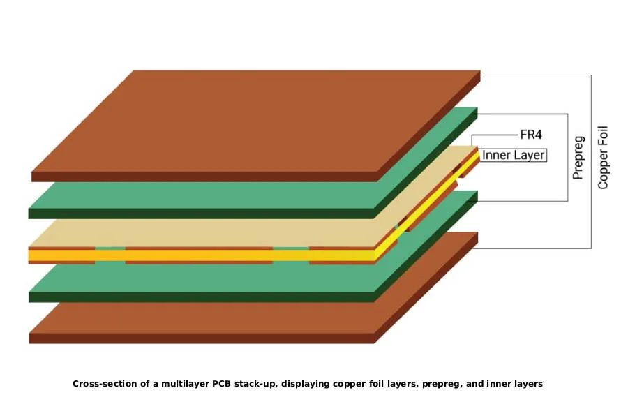
HDI technology, which enables more components to fit into smaller spaces through microvias and finer traces, is driving a rethinking of ground plane partitioning. In HDI designs, ground planes are often layered across multiple levels of a multi-layer PCB, requiring precise partitioning to manage return paths for high-speed signals.
Consider a smartphone PCB using HDI with trace widths as small as 3 mils (0.076 mm). Without proper ground plane partitioning, signal return paths can become inconsistent, leading to impedance mismatches and signal degradation at frequencies above 5 GHz. The trend is toward using continuous ground planes beneath critical signal layers while partitioning less critical areas to save space, balancing performance with manufacturability.
3. Ground Plane Partitioning in Flexible PCBs
Flexible PCBs are gaining popularity in wearable devices, medical equipment, and automotive applications due to their ability to bend and conform to unique shapes. However, their dynamic nature introduces new challenges for ground plane partitioning. Unlike rigid PCBs, flexible boards experience mechanical stress, which can affect ground plane integrity over time.
The emerging trend is to use segmented ground planes with reinforced connections to maintain signal integrity under flexing conditions. For instance, in a wearable fitness tracker, the ground plane might be split into smaller, localized sections to reduce stress points while ensuring a low-impedance path for signals. Additionally, designers are incorporating mesh-style ground planes in flexible PCBs to improve flexibility without sacrificing EMI shielding.
4. Adaptation for 3D PCBs and Stacked Designs
3D PCBs, which stack multiple layers or boards to save space, are becoming a game-changer in compact electronics. Ground plane partitioning in these designs must account for vertical signal paths and inter-layer connectivity. The trend is toward creating dedicated ground planes for each stacked layer while using vias to establish controlled return paths.
In a 3D PCB for a drone controller, for example, partitioning the ground plane between power, control, and communication layers can reduce crosstalk by up to 25% at operating frequencies of 2.4 GHz. This approach ensures that high-speed signals traveling vertically through vias have a stable reference plane, minimizing signal loss in the future of electronics.
5. Embedded Components and Ground Plane Optimization
Embedding components like capacitors, resistors, and even active devices within the PCB substrate is a growing trend in advanced PCB design. This technique reduces board size and improves performance by shortening signal paths. However, it complicates ground plane partitioning since embedded components often require localized ground references.
The future lies in adaptive ground plane designs that dynamically adjust to the placement of embedded components. For example, in a multi-layer PCB with embedded decoupling capacitors, a small isolated ground plane section beneath the capacitor can reduce parasitic inductance by 15-20% compared to a shared ground plane. This trend is particularly relevant for high-speed applications like 5G communication modules, where every nanosecond of signal delay matters.
Challenges and Solutions in Modern Ground Plane Partitioning
While emerging trends offer exciting possibilities, they also bring challenges that engineers must address to ensure reliable performance in advanced PCB design.
Challenge 1: Balancing Partitioning with Signal Integrity
Over-segmenting a ground plane can disrupt signal return paths, leading to increased impedance and signal distortion. For high-speed designs operating at 10 Gbps or higher, this can result in bit error rates exceeding acceptable limits (e.g., 10^-12).
Solution: Use simulation software to model ground plane splits and predict their impact on signal integrity. Additionally, maintain a continuous ground plane under critical high-speed traces while partitioning only non-critical areas.
Challenge 2: Managing EMI in Compact Designs
As PCBs become smaller with HDI and embedded components, EMI risks increase due to closer proximity of signals and power lines. Poor ground plane partitioning can exacerbate this issue, especially in flexible and 3D PCBs.
Solution: Incorporate shielding techniques, such as adding guard traces or using solid ground planes as EMI barriers. For instance, placing a solid ground plane between a noisy power layer and a sensitive signal layer can reduce EMI by up to 40% in compact designs.
The Role of Ground Plane Partitioning in the Future of Electronics
Ground plane partitioning is set to play a pivotal role as electronics continue to evolve. With the rise of 5G, Internet of Things (IoT), and autonomous systems, PCBs must handle higher data rates, denser layouts, and stricter EMC requirements. Here’s how ground plane partitioning ties into these broader trends:
- 5G and High-Speed Communication: Partitioned ground planes will be essential for isolating high-frequency signals (up to 28 GHz or higher) in 5G devices, ensuring minimal interference and stable performance.
- IoT and Wearables: Flexible PCBs with optimized ground planes will support the compact, lightweight designs needed for IoT sensors and wearable tech.
- Automotive Electronics: In electric vehicles and autonomous systems, 3D PCBs with carefully partitioned ground planes will manage complex power and signal requirements while meeting stringent safety standards.
Best Practices for Ground Plane Partitioning in Advanced PCB Design
To stay ahead in the future of electronics, engineers should adopt the following best practices for ground plane partitioning:
- Prioritize Signal Return Paths: Always ensure that high-speed signals have a continuous ground plane beneath them to minimize impedance discontinuities.
- Use Simulation Tools: Leverage advanced software to simulate ground plane splits and their impact on noise, EMI, and signal integrity before manufacturing.
- Minimize Ground Loops: Connect partitioned ground sections at a single point to avoid loops that can introduce noise.
- Adapt to Design Type: Tailor partitioning strategies to the specific needs of flexible PCBs, 3D PCBs, or HDI layouts, considering mechanical and electrical constraints.
- Test and Iterate: Prototype and test designs to validate ground plane performance under real-world conditions, especially for high-frequency or high-density applications.
Conclusion: Preparing for the Future of Ground Plane Partitioning
The future of ground plane partitioning is bright, with emerging trends like smarter segmentation, integration with HDI, and adaptation for flexible and 3D PCBs paving the way for more efficient and reliable electronics. As the industry moves toward the future of electronics, mastering these techniques will be crucial for engineers working on advanced PCB design. By staying informed about these trends and adopting best practices, designers can create boards that meet the demands of high-speed, high-density, and compact applications.
At ALLPCB, we’re committed to supporting engineers with the tools and resources needed to navigate these advancements. Whether you’re designing for 5G, IoT, or automotive applications, understanding and implementing effective ground plane partitioning will ensure your projects succeed in the ever-evolving world of electronics.
 ALLPCB


