 ALLPCB


Are you a hobbyist looking to take your DIY PCB projects to the next level with advanced design techniques? Incorporating blind vias into your printed circuit boards (PCBs) can help you achieve high-density designs and improve performance, even in a home setup. In this comprehensive guide, we'll walk you through the essentials of using blind vias in DIY PCB projects, from understanding their purpose to practical tips for home manufacturing. Whether you're exploring multilayer PCB designs at home or etching blind vias for compact layouts, we've got you covered with actionable advice and detailed insights.
What Are Blind Vias and Why Use Them in DIY PCB Projects?
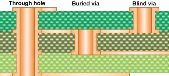
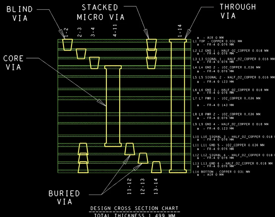
Blind vias are a type of vertical interconnect access (VIA) in a PCB that connect an outer layer to one or more inner layers without passing through the entire board. Unlike through-hole vias, which go all the way from the top to the bottom of the board, blind vias are only visible on one side, making them ideal for high-density designs where space is limited.
For hobbyists working on advanced PCB designs, blind vias offer several benefits. They allow you to pack more components into a smaller area by freeing up space on the opposite side of the board. They also help reduce signal interference by shortening the path signals need to travel, which is critical for high-speed applications. For instance, in a design operating at frequencies above 1 GHz, shorter vias can minimize signal loss, potentially reducing attenuation by up to 20% compared to longer through-hole vias.
In this blog, we'll dive deep into how you can integrate blind vias into your DIY PCB with blind vias, explore home PCB manufacturing techniques, and provide tips for advanced PCB design for hobbyists. Let's get started on elevating your projects with multilayer PCB at home.
Understanding the Basics of Blind Vias in PCB Design
Before jumping into the practical aspects of etching blind vias or building a multilayer PCB at home, it's important to grasp the fundamentals. Blind vias are typically created using precise drilling techniques, often with lasers in professional settings, to ensure they stop at the correct inner layer. The diameter of these vias can be as small as 0.1 mm (4 mils), allowing for incredibly compact designs.
The primary advantage of blind vias in DIY PCB projects is their ability to support high-density interconnects (HDI). This is especially useful for hobbyists working on projects like miniature IoT devices or compact wearable electronics, where every square millimeter counts. Additionally, blind vias can improve the impedance control of your board. For example, maintaining a consistent impedance of 50 ohms for high-speed signals is easier with shorter blind vias, as they reduce parasitic inductance compared to through-hole vias.
However, blind vias come with challenges, especially for home manufacturing. The precision required to drill to a specific depth without penetrating other layers can be tricky without specialized equipment. Plus, the cost of manufacturing boards with blind vias is often higher due to the complexity involved. As a hobbyist, you'll need to weigh these factors against the benefits for your specific project.
Benefits of Using Blind Vias in Advanced PCB Design for Hobbyists
Let's explore the key reasons why blind vias are worth considering for your advanced PCB designs:
- Space Efficiency: Blind vias don't occupy space on the opposite side of the board, allowing you to place components or traces there. This can reduce board size by up to 30% in some multilayer designs.
- Signal Integrity: Shorter vias mean less signal distortion. For high-speed designs, this can improve performance by maintaining signal rise times as low as 100 picoseconds.
- Layer Optimization: In a multilayer PCB at home, blind vias let you connect specific layers without affecting others, giving you more flexibility in routing complex circuits.
- Reduced EMI: Electromagnetic interference (EMI) is minimized with shorter interconnects, which is crucial for RF or wireless projects where interference can degrade performance by 10-15%.
These advantages make blind vias a powerful tool for hobbyists pushing the boundaries of DIY PCB projects. However, achieving these benefits at home requires creative solutions and careful planning, which we'll cover next.
Challenges of Home PCB Manufacturing with Blind Vias
While blind vias are a game-changer for advanced designs, they pose unique challenges for home PCB manufacturing. Here are some hurdles you might face and how to approach them:
- Drilling Precision: Creating blind vias requires stopping the drill at a specific depth, which is difficult with standard hobbyist tools. A drill press with a depth stop can help, but it won't match the precision of professional laser drilling, where depth control is within 0.01 mm.
- Plating Issues: After drilling, the via needs to be plated to ensure conductivity. At home, achieving uniform plating inside a blind via is tough without electroless plating solutions, which can be costly and hazardous to handle.
- Cost: Even if you're outsourcing the manufacturing of your PCB, blind vias can increase costs by 50-100% compared to standard through-hole vias due to additional processing steps.
- Testing and Repair: Since blind vias are hidden from one side, troubleshooting connectivity issues becomes harder. You might need an X-ray inspection tool, which is beyond the reach of most hobbyists.
Despite these challenges, there are ways to incorporate blind vias into your DIY PCB with blind vias by adapting your design and manufacturing approach. Let's explore some practical methods.
How to Incorporate Blind Vias in DIY PCB Projects at Home
Creating a multilayer PCB at home with blind vias might seem daunting, but with the right techniques and mindset, it's achievable for advanced hobbyists. Here's a step-by-step guide to get you started with home PCB manufacturing:
Step 1: Design Your PCB with Blind Vias in Mind
Use PCB design software that supports multilayer layouts and via customization. Define the layers you want to connect with blind vias and specify their start and end points. Keep via diameters small, ideally between 0.2 mm and 0.3 mm, to minimize drilling challenges. Ensure that your design adheres to a minimum pad size of 0.5 mm around the via to account for alignment errors during manufacturing.
Step 2: Choose the Right Materials
For multilayer PCB at home, select thin laminate materials (e.g., FR-4 with a thickness of 0.2 mm per layer) to make drilling easier. Thinner layers reduce the risk of overshooting your target depth when creating blind vias. Also, ensure you have access to copper-clad boards and prepreg for bonding layers together.
Step 3: Drilling Blind Vias with Precision
Etching blind vias at home requires a steady hand and the right tools. A mini CNC machine or a drill press with a depth stop can help control the drilling depth. Start with a small pilot hole (0.1 mm) and gradually widen it to your desired size. Measure the depth frequently with a caliper to avoid drilling too deep. For a 4-layer board, if you're connecting layer 1 to layer 2, stop drilling at approximately 0.3 mm, assuming each layer and prepreg is 0.2 mm thick.
Step 4: Plating the Vias
Plating blind vias at home is tricky but possible with conductive ink or epoxy. Apply the conductive material inside the via using a fine syringe, ensuring it makes contact with the target layers. Alternatively, small rivets or wire can be inserted and soldered to mimic plating, though this method is less reliable for high-speed signals due to potential impedance mismatches.
Step 5: Assemble and Test Your Board
Once your vias are in place, bond the layers using heat and pressure (a household iron can work for small boards). After assembly, test for continuity between the connected layers using a multimeter. If a blind via fails to connect, you may need to rework the design or consider outsourcing this step for better precision.
Tips for Successful Advanced PCB Design for Hobbyists
To make the most of blind vias in your DIY PCB projects, keep these practical tips in mind:
- Start Simple: If you're new to multilayer designs, begin with a 4-layer board before moving to 6 or 8 layers. This reduces complexity and cost while you learn to handle blind vias.
- Optimize Routing: Place blind vias strategically to shorten signal paths. For instance, in a high-speed USB design, position vias near the connector to maintain a signal delay below 50 picoseconds.
- Use Simulation Tools: Software with signal integrity analysis can predict how blind vias affect performance. Look for free or open-source tools to simulate impedance and crosstalk before manufacturing.
- Consider Outsourcing: If home PCB manufacturing of blind vias proves too challenging, partner with a reliable fabrication service for the drilling and plating steps. Many services offer affordable prototyping for small runs, often under $50 for a batch of 5 boards.
- Document Everything: Keep detailed notes on your drilling depths, via sizes, and plating methods. This helps troubleshoot issues and refine your process for future projects.
Real-World DIY PCB Project Example with Blind Vias
To illustrate the power of blind vias, consider a project like a compact Wi-Fi module for IoT applications. In a 4-layer board design, you could use blind vias to connect the top layer (where the antenna resides) to an inner ground plane on layer 2, while leaving layers 3 and 4 free for power distribution and additional routing. This setup reduces the board's footprint to just 20 mm x 20 mm, a 25% size reduction compared to a 2-layer design with through-hole vias. The blind vias also help maintain a stable 50-ohm impedance for the antenna trace, ensuring reliable wireless performance at 2.4 GHz.
By etching blind vias between layers 1 and 2, you avoid cluttering the bottom layer with unnecessary holes, allowing for a cleaner layout of surface-mount components. While drilling and plating at home might take trial and error, the end result is a professional-grade board that rivals commercial designs.
Conclusion: Elevate Your DIY PCB Projects with Blind Vias
Incorporating blind vias into your DIY PCB projects opens up a world of possibilities for advanced designs. From saving space to enhancing signal integrity, these specialized vias are a must-have for hobbyists tackling high-density or multilayer PCB at home. While home PCB manufacturing of blind vias presents challenges like drilling precision and plating difficulties, with the right tools and techniques, you can achieve impressive results. Whether you're etching blind vias for a tiny IoT device or exploring advanced PCB design for hobbyists, the effort pays off in creating compact, high-performance boards.
Start small, experiment with different methods, and don't hesitate to leverage professional fabrication services when needed. With patience and practice, you'll master the art of using blind vias to push your DIY PCB projects to new heights. Keep innovating, and watch your designs come to life with the power of advanced multilayer techniques!


